Microstructure and Electromigration Properties of Submicron Al(.5%Cu) Lines
- PDF / 1,045,007 Bytes
- 7 Pages / 414.72 x 648 pts Page_size
- 32 Downloads / 432 Views
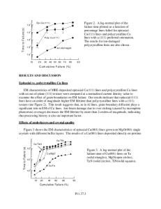
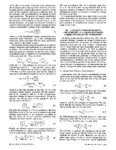
were attached to two pads at opposite ends of the structure. Each 50-line unit consisted of lines of all one width, either 0.3, 0.5, or 0.8 pm. The TEM sample preparation consisted in a two-step etch using first a nitric/acetic/hydrofluoric acid etch followed by EDP (ethylene diamine pyrocatechol). The EDP is a slow etch and stops on the Si0 2 leaving a SiO2 membrane with the metal lines intact on top. The 2000A thick lines were fabricated on a SiNX membrane on a Si wafer instead of Si0 2. 1500A of (Si-rich) SiNZ was deposited on a Si wafer by LPCVD and 300x300 pm windows were etched in the Si substrate using EDP. 2000A of Al(.5%Cu) was then blanket deposited and e-beam patterned into testers consisting of 5 parallel lines of width 0.2, 0.4, 0.6, 0.8, and 1.0 pm, and each 300 pm long. All five lines were connected in parallel to two pads. For both samples, passivated and unpassivated lines were studied. The 1000iA of Si02 passivation was deposited in an Electrotech plasma-enhanced (PE) silane-based oxide tool, at a temperature of 300 C. For the microstuctural evolution studies, the samples were annealed in a temperature range of 400-525 C. Electromigration was studied under the accelerated conditions of >200 C and 2 - 3 x 10⁶ A/cm 2 . The studies were performed using a JEOL 2000 FX TEM. For the in situ experiments, a stage designed by Gatan Inc. was used which allowed for heating and passing current simultaneously. Results were recorded using conventional electron micrograph techniques as well as real-time motion videos. RESULTS AND DISCUSSION Temperature Cycling We report on the microstructure of the lines for the case of as-deposited and annealed under various conditions. The lines are characterized in terms of the degree to which they are "bamboo", meaning all grain boundaries are parallel to each other and perpendicular to the direction of current flow along the line. Our findings are considered in terms of 2D grain growth simulations of thin films and lines [1,7]. Statistical information was obtained for each linewidth by making observations on various lines chosen randomly from the test structure. We first give the results of annealing the 4000 A passivated lines. The 0.8 pm lines had the most complex grain boundary (gb) structure, due to their being the widest lines cut through a film of comparable grain size. Rather than a single grain throughout the width of these lines as for bamboo, there were usually multiple grains throughout the width at a given site. Only approximately 30% of the gb's went across the full width, and of these < 10% were perpendicular to the length of the line. The remaining 70% of the gb's were associated with multiple grains across the width. The larger grains were 1-2x the linewidth, but there were many smaller grains ( 10 pm. Grain growth in the lines was much less than in the pads and only slightly greater than for the lower temperature anneals. However, the grain boundary arrangement in the lines became very close to bamboo. A 525 C anneal is sufficient to break up most small gr
Data Loading...