Localized epitaxy of diamond on (100) silicon
- PDF / 951,193 Bytes
- 5 Pages / 576 x 792 pts Page_size
- 2 Downloads / 367 Views
M. G. Jubber, M. Liehr, and J. I. B. Wilson Department of Physics, Heriot-Watt University, Riccarton, Edinburgh EH14 4AS, United Kingdom (Received 13 June 1994; accepted 30 August 1994)
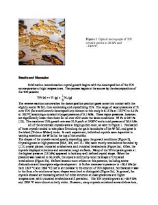
Diamond films exhibiting contiguous epitaxial crystallites ( ~ 3 - 4 /mm) have been grown on single crystal (100) silicon by 2.45 GHz microwave plasma deposition. The diamond films were deposited by a three-step process. In the initial stage the silicon wafer was pretreated for 3 h in a 1.8% methane in hydrogen plasma at low pressure. The subsequent nucleation stage was performed, under identical processing conditions, except that a dc bias of —340 V was applied for 25 min. During this period the current increased from 38 mA at the start to 102 mA at the end of the bias. The final growth stage was performed, with an earthed substrate, utilizing a carbon monoxide/methane/hydrogen gas mixture whose composition is conducive to uniformly faceted (100) diamond growth. Scanning electron micrographs showed that a large fraction of the (100) faces of the diamond crystallites are aligned with the (100) plane of the underlying silicon lattice with the crystallite edges parallel to the (110) direction. Raman scattering was used to confirm this finding by measuring the angular dependence of the Raman backscattering intensity at 1332 cm" 1 using plane polarized excitation of individual crystallites within the diamond films.
I. INTRODUCTION Heteroepitaxial growth of diamond on silicon represents an important milestone in the development of diamond electronics. However, the problems in devising a method for large area epitaxy are formidable. The fundamental difficulties are associated with the large lattice mismatch and the high surface energy of diamond compared to silicon. Despite these difficulties, the fact that carrier mobilities are enhanced in oriented films1 makes it imperative that simple procedures for diamond heteroepitaxy are developed if the applications of diamond films are to be fully exploited. The published procedures2"13 for epitaxial growth on (100) silicon arise mainly from two research groups. In the pertinent publications arising from the groups of Klages and coworkers2"6 and Stoner and co-workers,7"12 the process entails three stages comprising (i) an initial pretreatment process, (ii) a bias-enhanced nucleation, and (iii) growth under specific plasma conditions. However, the nature and role of the pretreatment procedure for the two groups is different. In one case2 the wafer is subject to a pure hydrogen plasma for a short time in order to remove the surface oxide, while Wolter et al.n use a methane/hydrogen plasma for a longer time in order to form a surface layer of silicon carbide. The subsequent
a)
Present address: Motorola Ltd., East Kilbride G75 0TG, United Kingdom. J. Mater. Res., Vol. 9, No. 12, Dec 1994 http://journals.cambridge.org
Downloaded: 31 Mar 2015
bias-enhanced nucleation (BEN) step, employed in both cases, eliminates the need for surface abrasion which is inimical to epitaxial growth. This BEN treat
Data Loading...