UHV STM of Cesium on Oxygenated Epitaxial Diamond (100) Films
- PDF / 1,739,487 Bytes
- 4 Pages / 414.72 x 648 pts Page_size
- 114 Downloads / 401 Views
Mat. Res. Soc. Symp. Proc. Vol. 509 01998 Materials Research Society
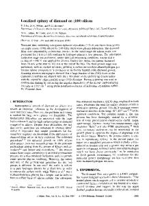
Figure 1. An atomic resolution UHV STM image of a CVD diamond (100) epitaxial film before Cs and 02 deposition, showing a (2xl) dimer reconstruction. respectively. Diborane was introduced at a concentration of 3 ppm relative to hydrogen in order to grow a conducting p-type film. The tungsten filament temperature was 2200 °C. The growth experiment was terminated by first shutting off only the methane flow while maintaining the sample, filament, and H 2 settings for 2 minutes. Then the filament, sample heater and H2 flow were turned off in that order. After growth, Cs was deposited on the surface using an SAES Getters Cs dispenser at a pressure : 10-9 Torr. After the Cs getter was turned off and cooled to room temperature, the diamond surface, also at room temperature, was then exposed to 02 at a pressure of 2x10"7 Torr for 100 seconds (approximately 10 L ). The STM images were obtained in UHV at a pressure ! 10-1 Torr using an Aris 5000 UHV compatible STM from Burleigh Instruments, Inc. Tunneling currents of approximately 0.1 nA and sample bias of ±7V were used to obtain atomic resolution. RESULTS AND DISCUSSION After growth, the epitaxial film appears smooth and transparent to the naked eye. We have found that further investigation with a scanning electron microscope (SEM) shows a featureless surface. Figure 1 shows an atomic resolution UHV STM image of the diamond (100) epitaxial film before Cs and 02 deposition showing a (2xl) dimer reconstruction of the surface [5]. Single steps are observed consisting of atomic planes with dimer rows rotated in the x-y plane 900 relative to the dimer rows in the upper or lower atomic planes. Figure 2 shows a large scale STM image of the same diamond film after Cs and 02 deposition obtained using a negative tip bias with respect to the sample. The sub-monolayer of adsorbates are distributed evenly over the diamond (100) surface and appear as round bright structures in the topographic images. Figures 3(a)-(e) show a series of atomic resolution UHV STM images taken of this same area. The images shown in Figs. 3(b)-(e) were taken one after the other using positive and negative tip voltages with respect to the sample. It is well known that with a negative tip bias, electrons will tunnel from the metal tip into empty electron states of the sample surface. Conversely, with a positive tip bias the electrons will tunnel from the filled electron states of the sample surface to
162
Figure 2. Large scale UHV STM image of the diamond (100) film after Cs and 02 deposition. A sub-monolayer of adsorbates is observed with a tip bias of-7V and a tunneling current of 0.1 nA.
Figure 3(a)-(e). STM topographs of diamond (100) after Cs and 02 exposure. Tip bias of ±7v and tunneling currents of 0.1 nA were used. These figures show the adsorbates' dependence on tip polarity. the metal tip [6]. This technique of changing the tip bias from one scan to the next is a very useful way of identifying adsorbates on a semiconductor surface
Data Loading...