Low temperature flash light curing of spray coated zirconium oxide gate dielectric for flexible, fully patterned and low
- PDF / 1,908,881 Bytes
- 6 Pages / 612 x 792 pts (letter) Page_size
- 56 Downloads / 306 Views
Low temperature flash light curing of spray coated zirconium oxide gate dielectric for flexible, fully patterned and low voltage operated organic thin film transistor
1 1 Sudipta K. Sarkar and Dipti Gupta 1 Department of Metallurgical Engineering and Materials Science, Indian Institute of Technology Bombay, Mumbai, Maharashtra 400076, India.
ABSTRACT In this work, we present low temperature flash light based curing of spray coated high-k zirconium oxide (ZrOx) thin film to realize low voltage operated flexible and fully patterned organic thin film transistors (OTFTs). A simple sol-gel technique was followed to prepare ZrOx from a zirconium complex. By spraying the precursor solution onto substrate through shadow mask, a patterned film was obtained. On the other hand subsequent flash light curing of the coated film not only reduced processing time but also allowed us to fabricate device on polymeric flexible substrate. Spectroscopic analysis confirmed formation of ZrOx film from the solution of zirconium complex. Finally as prepared ZrOx was used as gate dielectric layer in OTFT structure to keep operating voltage as low as -3V. Flexible polyethylenetrephthalate (PET) sheet was used as flexible substrate and pentacene was used as organic active layer. Each and every layer was deposited through metal made shadow mask to develop fully patterned OTFT. Field effect mobility and ON/OFF ratio of as fabricated transistor was found to be as high as 1.2 cm2V-1S-1 and 105 respectively.
INTRODUCTION Organic thin-film transistors (OTFTs) are of research interest owing to their potential for use in flexible, large area, and high volume electronic applications such as display backplanes, sensor networks, and disposable electronics [1]. To perceive such applications, several reports have addressed design and processing strategies of organic semiconductor with improved OTFT performance [2][3]. However, development of reliable gate dielectrics is equally significant for practical applications. In particular, for low voltage operation, use of high K materials as gate dielectric in transistor structure has become a routine practice now [4][5][6][7]. However, as OTFT is potentially targeted for low cost, large area, flexible electronic applications, use of high K materials in OTFTs is limited by several factors. For example, sputtering method which is mostly followed to deposit dielectric material, is a high vacuum based expensive technique and therefore it is not suitable for low cost applications. Although an alternative spin coating method of preparing film from sol-gel prepared dielectric, is a non-vacuum technique, subsequent high temperature annealing step hinders it applications on flexible substrates (low glass transition temperature) [4][8]. Therefore development of inexpensive, fast, large-scale and low temperature processing methods for gate dielectrics is still obstacle preventing commercialization. In addition, patterning of dielectric layer which is also of much importance to develop fully patterned
Downloaded from htt
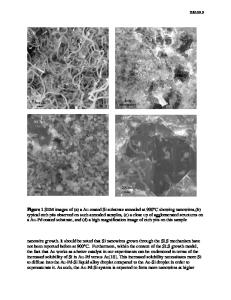
Data Loading...