Low-temperature growth of HfO 2 dielectric layers by Plasma-Enhanced CVD
- PDF / 171,542 Bytes
- 6 Pages / 612 x 792 pts (letter) Page_size
- 8 Downloads / 281 Views
E3.15.1
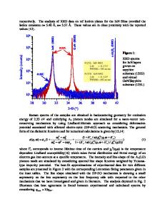
Low-temperature growth of HfO2 dielectric layers by Plasma-Enhanced CVD M. Losurdo, M.M. Giangregorio, M. Luchena, P. Capezzuto, G. Bruno, IMIP-CNR and INSTM, Department of Chemistry, University of Bari, via Orabona, 4 – 70126 Bari, Italy D. Barreca, A. Gasparotto, E. Tondello ISTM-CNR and INSTM, Department of Chemistry, University of Padova, via Marzolo 1, – 35131 Padova, Italy ABSTRACT HfO2 dielectric layers have been grown on p-type Si(100) by plasma enhanced chemical vapor deposition (PE-CVD), using Ar-O2 plasmas and hafnium(IV) tetra-t-butoxide as precursors. In-situ control of the plasma phase is carried out by optical emission spectroscopy (OES) and quadrupolar mass spectrometry (QMS). Structural and optical properties of the HfO2 layers and of the HfO2/Si interface are investigated by spectroscopic ellipsometry (SE) in the photon energy range 1.5 – 6.0 eV.. SE data are corroborated by results obtained from glancing incidence X-ray diffraction (GIXRD), atomic force microscopy (AFM) and X-ray photoelectron spectroscopy (XPS). The effect of the substrate temperature (RT-250°C) and precursor flow on the thickness of interfacial SiO2 layer and on the HfO2 microstructure is investigated. The growth dynamics of HfO2 film and SiO2 interface layer is also discussed. INTRODUCTION High-K materials have been largely investigated in the last years to satisfy microelectronic industry requirements. The expansion of technological market and the need of faster circuits in the transmission of informations requires a rapid shrinking of the transistor size. To this aim, the use of dielectric materials with a permittivity higher than that of conventional SiO2 (K=3.9) is the key factor for the scaling of silicon based metal-oxide-semiconductor field effect transistor (MOSFET) In this context, HfO2 is regarded as the most reliable oxide material because of its high dielectric constant (>25), large band gap (∼6 eV), and good interface stability with Si [1]. HfO2 films can be obtained by several techniques, such as physical vapor deposition (PVD,, sputtering [2], and chemical vapor deposition (CVD) [3,4]. CVD methods represent a valuable alternative over other synthesis techniques because they are more compatible with CMOS processing. In fact, CVD processes offer a number of benefits, such as good conformal coverage, thickness control, high wafer throughputs and compatibility with new 300-mm wafer processing guidelines. Among the various CVD techniques, plasma enhanced CVD enables higher deposition rates even at low substrate temperatures, which can prevent the diffusion of shallow junctions and reduce thermal strains leading to defect generation. In the deposition of all thin gate dielectrics, the interface with Si plays a key role in determining the overall electrical properties. Many of high-K metal oxide systems have unstable interfaces with Si due to undesired reactions resulting in the presence of interfacial layers, whose formation is related to the reaction kinetics associated with film growth. The suppression of Si
Data Loading...