Properties of InN layers grown by High Pressure CVD
- PDF / 175,931 Bytes
- 6 Pages / 612 x 792 pts (letter) Page_size
- 60 Downloads / 453 Views
0955-I08-04
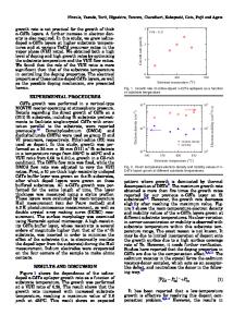
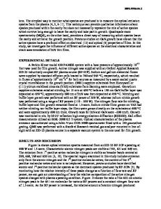
Properties of InN layers grown by High Pressure CVD Mustafa Alevli1, Goksel Durkaya1, Ronny Kirste1,2, Aruna Weesekara1, Unil Perera1, William Fenwick3, Vincent Woods3, Ian T. Ferguson3, Axel Hoffmann2, and Nikolaus Dietz1 1 Department of Physics & Astronomy, Georgia State University, Atlanta, GA, 30303 2 Department of Physics, Technical University Berlin, Berlin, D-10623, Germany 3 School of ECE, Georgia Institute of Technology, Atlanta, GA, 30332 ABSTRACT Indium nitride (InN) and indium-rich group III-nitride alloys are promising for a variety of advanced optoelectronic device applications. Embedded indium-rich alloys in wide-bandgap group III-nitrides, e.g. GaAlN, are essential for the fabrication of monolithic integrated light emitting diodes that are tunable in the whole visible spectral region, as well as advanced high speed optoelectronics for optical communication operating. The present limitation in the formation of embedded indium-rich group III-nitrides arise from the dissimilar processing windows in growth of GaAlN versus InGaN at traditional low-pressure growth techniques. In the work, a novel "high-pressure chemical vapor deposition" (HPCVD) system is employed, which enables the control of the partial pressures of the InN constituents at processing conditions similar to GaN. The structural analysis of InN layer deposited by HPCVD revealed high-quality, single phase InN(0002) layers with full width half maximum (FWHM) around 385 arcsec for layers grown on GaN/sapphire templates. Raman, transmission and IR reflection spectroscopy are used to study the structural and optical properties of InN thin films grown on sapphire (0001) and GaN/sapphire substrates. The modeling of the transmission spectra by a Lorentzian oscillator model indicates an absorption edge between 1.5 eV and 1.1 eV, with two absorption centers at 1.2 eV and 0.8 eV. The strength of these two absorption centers correlates with the employed precursor ratio, the origin of which is not completely understood at present. The free carrier concentrations in the layers are presently in the mid 1019 to low 1020 cm-3, as determined by IR-reflectance and Raman A1 analysis. A reduction of external impurities will be required to further improve the InN material quality. The processing window used for InN growth by HPCVD enables for the first time the fabrication of embedded indium-rich group III-nitride heterostructures. INTRODUCTION Group III-nitride compound semiconductors alloyed from their binaries AlN, GaN, and InN enable unique device structures ranging from IR to the deep UV wavelength range. While the materials quality for GaN-AlN compounds and alloys are already at a device fabrication level, the physical properties of InN and indium-rich alloys are still strongly process dependent and far from being integrated in GaAlN wide bandgap heterostructures[1-2]. At present, two of the most severe problems are related to the surface termination of indium-rich InGaN layers and secondly the large thermal decomposition pressures in InN which
Data Loading...