Low Temperature Oxidation of Silicon After Copper Ion Implantation
- PDF / 972,884 Bytes
- 5 Pages / 414.72 x 648 pts Page_size
- 77 Downloads / 378 Views
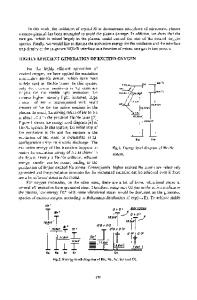
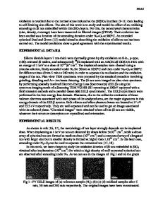
samples were pulse-biased to -2 kV with a pulse duration of 2 pts and a pulse off-time of 4 pts. Since the mean ion charge state for a copper plasma produced by a cathodic arc discharge is 2+, the mean ion energy during the implantation is 4 keV. Between bias pulses low energy deposition takes place with an average ion energy of 50 eV, which is the kinetic energy of ions produced by a cathodic arc discharge. At low doses (typically < 1016 /cm 2 ) alternating deposition and implantation leads to the formation of a very thin, compositionally uniform, intermixed layer of copper and silicon at the surface and a Gaussian implantation depth profile with a range and straggle of 7 nm and 3 nm respectively. At higher doses (typically >10 16 /cm 2 ) a film is formed at the substrate surface. The film is composed of an intermixed region of copper and silicon about 15 nm thick. The total implanted/deposited doses ranged from 1x10 16 /cm 2 - 50x101 6/cm 2, with ion current densities of 0.1 mA/cm 2. The implantation was done at a pressure below 10-6 Torr. Samples were measured by RBS after ion implantation and room-temperature aging in air. Backscattering analysis of the as-implanted samples displayed the expected Gaussian Cu profiles. There was no discernible silicon oxidation immediately after irradiation. Backscattering analysis [6] with 2.4 or 2.8 MeV 4 He2 ÷ ions was used to evaluate the sample composition after irradiation and to monitor the oxide growth. The analysis was performed using a solid-state detector, with a nominal resolution of better than 20 keV, positioned directly below the incident beam at a scattering angle of t170'. Experimental RBS spectra were simulated using the computer program RUMP [7]. The microstructure and phase formation in the implanted wafers were analyzed using Phase identification was cross-section-transmission-electron microscopy (XTEM). accomplished using selected-area diffraction (SAD). A JEOL JEM 200CX transmissionelectron microscope was used for analysis at an operating voltage of 200 kV. RESULTS AND DISCUSSION Figure 1 shows the backscattering spectrum and simulation for a Si substrate after room temperature implantation with 4x10 16 /cm 2 copper ions, and ambient aging for 8 months. There are two interesting points: 1) oxide growth, and 2) a splitting of the Cu profile. The RBS spectrum shows the presence of a thick 1.34 [tm layer of Si0 2 underneath the Cu-rich surface layer. Oxidation is quantified by simulation of the spectrum, and the oxide is found to have a composition of approximately stoichiometric Si0 2 . Previous reports stated that the silicon to oxygen ratio was 1:1.7 for room temperature oxidation of Cu 3 Si/Si structures [1]. Inspection of the implanted Cu profile shows that it is no longer Gaussian after aging. The Cu has redistributed into a stationary peak at the surface and a mobile Cu peak at depth. The second peak (in Fig. 1) appears at an energy equivalent to Cu at the depth of the Si0 2/Si interface; this peak suggests that the Cu segregates to the Si0 2 /Si inter
Data Loading...