Low Voltage Tunable One Dimensional Photonic Crystal with Large Air Defects
- PDF / 39,418 Bytes
- 4 Pages / 612 x 792 pts (letter) Page_size
- 95 Downloads / 244 Views
Low Voltage Tunable One Dimensional Photonic Crystal with Large Air Defects Yasha Yi, Peter Bermel, Kazumi Wada, Xiaoman Duan, John. D. Joannopoulos and Lionel. C. Kimerling Massachusetts Institute of Technology, 77 Massachusetts Avenue, Cambridge, MA 02139, U.S.A. ABSTRACT A one-dimensional Si/SiO2 photonic crystal with a large, tunable air defect cavity is fabricated. Multiple resonant modes are observed within the photonic band gap. The free spectral range (FSR) is large compared to other resonant structures, with more than 100nm bandwidth. Simultaneous low voltage tuning around two telecom wavelengths, 1.55µm and 1.3µm, is realized using electrostatic force. The whole process is at low temperature and can be CMOS compatible. Potential applications include switching, modulation, and wavelength conversion devices, particularly WDM devices.
INTRODUCTION Tunable photonic crystals are key devices for microphotonics, especially for future WDM applications [1,2]. Since the introduction of Photonic Band Gap structures (PBG) [3], also known as photonic crystals, new concepts and designs have been proposed, which could be the building blocks for photonic integrated circuits [4,5]. When defects are introduced into PBG materials, highly localized states, which confine light to within the defects, can be created [6,7]. The confinement of light to distances on the order of one wavelength will lead to large reduction of photonic circuit size and numerous useful devices, especially for Si microphotonics[8,9]. Realization of a tunable photonic crystal makes it an active component, which could play a key role in switching, modulation and wavelength conversion. Here we demonstrate a tunable one-dimensional photonic crystal with a “large” air defect cavity (with a size of several operating wavelengths) in silicon based PBG materials. Multiple localized resonance modes are observed within the photonic band gap at 1.402µm, 1.582µm, 1.792µm and 2.072µm. The observed photonic band gap is from 1.19µm to 2.18µm, which has 1000nm bandwidth. The free spectral range (FSR) is larger than 100nm. Employing electrostatic force, simultaneous low voltage tuning of two localized modes around two telecom wavelengths, 1.3µm and 1.55µm, is achieved. At 10V, a mode shift of almost 60nm is also achieved. This is the lowest we have seen to date.
L3.3.1
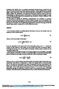
EXPERIMENTS The schematic illustration of the tunable PBG device is shown in Fig.1. We emphasize that, a) the whole process is CMOS compatible. b) low temperature process is preserved. Low temperature process reduces the film stress significantly, which is critical for the optical properties and polymer based materials can be incorporated into the process. Starting with (100) Si substrate(about 500um in thickness), the SiO2 layer is deposited by Plasma Enhanced Chemical Vapor Deposition(PECVD). Silicon layer is formed via e-beam deposition. After deposition of first several SiO2/Si pair layers, followed by another oxide layer by PECVD, Polyimide(PI) film is spin coated at various speed for different P
Data Loading...