Luminescence of Be-doped GaN layers grown by molecular beam epitaxy on Si (111)
- PDF / 205,784 Bytes
- 7 Pages / 612 x 792 pts (letter) Page_size
- 112 Downloads / 384 Views
Internet Journal Nitride Semiconductor Research
Luminescence of Be-doped GaN layers grown by molecular beam epitaxy on Si (111). F. J. Sánchez1, F. Calle1, M.A. Sanchez-Garcia1, E. Calleja1, E. Muñoz1, C. H. Molloy2, D. J. Somerford2, F. K. Koschnick3, K. Michael3 and J.-M. Spaeth3 1Dpt.
Ingeniería Electrónica, E.T.S.I. Telecomunicación, Politécnica, Ciudad Universitaria, of Physics and Astronomy, University of Wales, 3Fachbereich Physik, University of Paderborn, 2Department
(Received Friday, June 19, 1998; accepted Thursday, September 10, 1998)
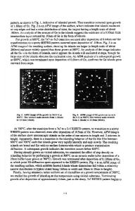
Low temperature photoluminescence spectra of Be-doped layers grown on Si (111) by molecular beam epitaxy have been analyzed. Emissions at 3.466 eV and 3.384 eV, and a broad band centered at 2.4-2.5 eV are observed. Their evolution with temperature and excitation power, and time resolved PL measurements ascribe an excitonic character for the luminescence at 3.466 eV, whereas the emission at 3.384 eV is associated with a donor-acceptor pair transition. This recombination involves residual donors and Be-related acceptors, which are located around 90meV above the valence band, confirming Be as the shallowest acceptor reported in GaN. The intensity of the band at 2.4-2.5 eV increases with the Be content. This emission involves a band of deep acceptors generated by Be complex defects, as suggested by the parameter g = 2.008 ± 0.003 obtained by photoluminescencedetected electron paramagnetic resonance.
1
Introduction
Controllable doping is a key issue for the fabrication of ultraviolet and blue emitters based on GaN alloys. Si and Ge have been successfully used for n-type doping [1]. P-type doping remains a challenge because of the high n-type residual background present in GaN, and the large ionization energy of acceptors (Mg, Zn, Cd) [2]. P-type GaN has been achieved by Mg doping of metalorganic chemical vapor deposition (MOCVD) [3] and molecular beam epitaxy (MBE) [4] layers. However, the large ionization energy of Mg (250 meV) [5] implies a low activation of the acceptor at room temperature. Hence, the search for shallower acceptors is still a matter of great importance. Be should be a shallower acceptor in GaN than Mg [6] [7] due to its large electronegativity and the absence of d-electrons [8]. Theoretical calculations suggest that Be behaves as a rather shallow acceptor in GaN [9], with a thermal ionization energy of 60 meV [10]. Nevertheless, experimental evidences point to the introduction of deep levels by Be doping in GaN. Several authors have reported a Be-related deep emission detected by photoluminescence (PL) in Be-doped [11] [12] and Be-implanted GaN [5], probably associated with the formation of complex defects. Salvador et al.
[13] observed a broad band centered at 390-420 nm, which is interpreted as a donor-acceptor emission involving Be acceptors, with an ionization energy of 250 meV. In this work, the optical properties of GaN:Be layers will be analyzed in order to determine the shallow acceptor level and study the generation of deep levels. 2
Experim
Data Loading...