Luminescent Nanometer-Sized Si Crystals Formed in an amorphous Silicon Dioxide Matrk by Ion Implantation and Annealing
- PDF / 1,214,009 Bytes
- 6 Pages / 414.72 x 648 pts Page_size
- 62 Downloads / 405 Views
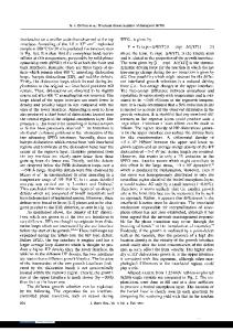
XPERIMENT Oxidized boron doped p-type Si wafers with a resistance of 0.01-0.02 ) cm were used. The orientation of the Si wafers was (100). Thermal oxide films on crystalline Si wafer were obtained through oxidation of the wafers by annealing at 1050 "C for 10 h in 60 % H 2 and 40 % 02 ambient. The oxide thickness was about 1.75 [tm. Si+-implantation was carried out at an energy of 1 MeV to a fluence of 2 x 10¹⁷ ions/cm 2 at room temperature. Heat treatments of the ion implanted specimens were carried out in vacuum using an electric oven. Photoluminescence spectra of specimens before and after annealing were measured at room temperature in a conventional way. An Ar-ion laser was used as an excitation source and the luminescence was detected by a cooled photomultiplier tube, employing the photon counting technique. Photoluminescence excitation spectroscopy was carried out using monochromatized light beams from a Xe-lamp as an excitation source and by detecting the luminescence through appropriate sharp-cut filters. The transmission electron micrographs were obtained by using a 300 keV electron microscope (H-9000NAR, Hitachi). For examining the microstructures of the specimens, the cross-sectioning method was employed. The specimens were first mechanically thinned down and then ion-milled to electron transparency using 5 keV Ar+-bombardment. RESULTS The luminescence spectra induced before and after annealing at 1100 "C for 90 min and 300 min of the specimens implanted to a fluence of 2 x 10¹⁷ ions/cm 2 at room temperature are shown in fig.1, in which each curve is normalized by the peak heights. As already reported' 6 , the shape of the luminescence spectra is complex because of interference effects. The primary luminescence band is peaked around 2.0 eV and 1.7 eV, respectively, similar to those having been observed before and after annealing at 1100 "C in silica glass specimens. As also reported previously"'"6 , the luminescence band around 2.0 eV, which is annealed after heating to about 600 "C, has been ascribed to the Si excess defects formed in Si0 2 or defects in SiOx. Moreover, the peak energies of the 2.0 eV luminescence depend on both the ion fluences and the temperature of substrates during implantation. In this paper we are concerned with the luminescence band around 1.7 eV, which is observed after annealing specimens at I100 "C. It is clear from fig. I that the shape of the luminescence spectra is not affected by the annealing time at 1100 "C. It is noted that the shape of the luminescence spectra after annealing is also found to be independent of the ion fluences and the temperature of substrates during ion implantation. However, the intensity of the luminescence is affected by the annealing time. The results of evolution and annealing of the luminescence band during annealing at I100 "C are shown in fig.2. Evidently the luminescence intensity grows and then decreases, as the annealing time increases. The maximum luminescence intensity is obtained with annealing for 90 min. The excitation spectra for the ph
Data Loading...