Mechanism of Dopant Activation Enhancement in Shallow Junctions by Hydrogen
- PDF / 476,600 Bytes
- 6 Pages / 612 x 792 pts (letter) Page_size
- 67 Downloads / 380 Views
E9.28.1
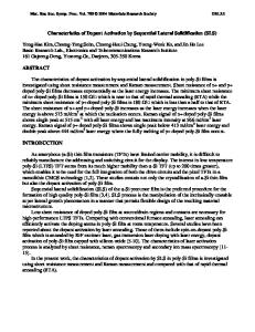
Mechanism of Dopant Activation Enhancement in Shallow Junctions by Hydrogen A. Vengurlekar, S. Ashok, Christine. E. Kalnas*, H. Win Ye* Department of Engineering Science, Pennsylvania State University, University Park, PA 16802 *Solid State Measurements Inc., Pittsburgh, PA 15275 ABSTRACT The ability to activate greater amounts of dopants is a significant challenge for the realization of shallow junctions in device scaling for Si CMOS technology. Dopant activation is difficult to achieve in shallow junctions due to higher concentrations of dopants and possible formation of dopant clusters. The high temperatures currently used to activate dopants result in increased junction depth and process integration issues with high-k dielectrics. However, lowering the annealing temperature results in lesser dopant activation and problems with transient enhanced diffusion. Our previous work reported on the enhancement of activation in boron implanted at a dose of 5E14/cm2 and annealed at temperatures of 450 oC and below, by the incorporation of atomic hydrogen introduced by exposing the substrate to a hydrogen plasma at 250 oC. In this work, further experiments have been carried out to get a better understanding of the mechanisms responsible for boron activation enhancement. Hydrogen-related activation was studied in boron, phosphorus and antimony implanted samples. The experimental results shed new light on the interactions among atomic hydrogen, point defects and dopants. INTRODUCTION The push toward shallow junctions is necessitated by the continual drive to smaller device dimensions. Avoiding transient enhanced diffusion (TED) is a major concern in shallow junction processing [1]. Another issue is obtaining a greater amount of dopant activation per unit volume, in order to keep pace with device scaling [2]. Approaches to tackling this problem involve annealing at very high temperatures for shorter durations (e.g. high ramp annealing, spike annealing, laser annealing and flash annealing) [3,4,5]. However, there are various problems associated with these techniques [5,6]. Another concern is that with the advent of high-k dielectrics, high-temperature annealing methods may not be suitable, because the thermal stability of most of the high-k dielectrics is limited. The usage of metal gates may also complicate the utilization of high-temperature annealing methods. Solid Phase Epitaxial Regrowth (SPER) is one dopant activation technique that does not involve high processing temperatures [7]. However, the occurrence of end-of-range (EOR) defects is a major disadvantage of this technique, as this causes leakage currents when the EOR defects are situated within the active layer of the device. Hence, a low-temperature activation technique that does not create excessive lattice damage would be advantageous. In our previous work, we reported on the enhancement of boron activation by hydrogen treatment [8]. A significant increase in boron activation after annealing was seen in hydrogenated Si samples that had been implanted with
Data Loading...