Thermal Stress Induced Void Formation in Narrow Passivated Cu Lines
- PDF / 1,902,859 Bytes
- 6 Pages / 420.48 x 639 pts Page_size
- 89 Downloads / 336 Views
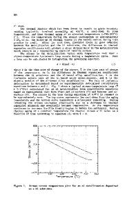
THERMAL STRESS INDUCED VOID FORMATION IN NARROW PASSIVATED Cu LINES D.D. Brown*, P. Borgesen*, D.A. Lilienfeld**, M.A. Korhonen* and C.-Y. Li* *Department of Materials Science & Engineering, Cornell University, Ithaca, NY 14853Facility, Cornell University, Ithaca, **National Nanofabrication New York 14853 ABSTRACT 0.75-3 Am wide copper lines encased in a thin adhesion layer of Al or Cr were passivated at 300°C and annealed at 400 0 C. The passivation was then removed and the lines examined in a scanning electron microscope. The development of thermal stress induced voiding was found to depend primarily on aging conditions and adhesion. INTRODUCTION Thermal stress induced voiding in narrow metal interconnects has become a serious concern in the microelectronics industry [1,2], both as a failure mechanism in itself and because the voids play a dominant role in subsequent electromigration failure [3,4]. Evidence suggests that the problem will worsen as line widths decrease [5,6]. Thermal stress induced void formation has been extensively studied in Al and Al alloys [1,2,5,7]. In industry, standard chip processing involves the high temperature passivation of narrow metal interconnects with a thick, rigid dielectric layer. Thermal expansion mismatch leads to large tensile stresses during subsequent cooling and the formation and growth of voids to relax these stresses [8,9]. It is believed that the high stress concentrations created by grain boundary sliding during cool-down are responsible for the nucleation of thermal stress voids [7,9]. These stress concentrations are greatest where the grain boundary intersects the interface between the metal line and the passivation and this is where voiding is most commonly observed. The dominant plastic deformation mechanism at a given temperature during cooldown depends on the strain rate (which depends on the cooling rate) and on the stress. In particular, there will be a region of cooling rates and temperatures in which grain boundary sliding is the dominant mechanism and void nucleation is favored. During a 'typical' cooldown of Al lines from 400 C to room temperature, for example, grain boundary sliding seems to occur at temperatures near 2000 [7). Once voids are nucleated, void growth will contribute directly to stress relaxation [8]. The growth of voids will, of course, generally be faster at elevated temperatures due to increased diffusivities. Cu has been suggested as an alternative to Al alloys for interconnect applications partly because of its higher melting temperature, resulting in a lower homologous temperature (and Mat. Res. Soc. Symp. Proc. Vol. 239. @1992 Materials Research Society
702
diffusivity) during and after cooling. Cu also has a smaller thermal mismatch with the passivation and substrate. However, the larger elastic modulus of Cu leads to a 50% larger stress increase per degree of cooling, resulting in higher overall stresses than for Al lines [10]. The adhesion of the passivation layer to the metal line is an important parameter in thermal stress voi
Data Loading...