Memory Effects of Ion-Beam Synthesized Ge and Si Nanoclusters in Thin SiO 2 - Layers
- PDF / 1,721,751 Bytes
- 5 Pages / 414 x 635.4 pts Page_size
- 99 Downloads / 331 Views
Rossendorf. e.V., PO Box 510119, D-01314 Dresden, Germany
Tel: ++49 (0)351 260 3036, Fax: ++49 (0)351 260 3285, email: [email protected] b Zentrum fWr Mikroelektronik Dresden GmbH, GrenzstraBe 28, D-01 109 Dresden, Germany Abstract: Nanocluster memories are promising for future non-volatile memory applications. In this work thin Si0 2 films were implanted with Ge+ and Si+ and annealed subsequently. Charge storage effects of the MOS capacitors have been studied through I-V and high frequency C-V measurements. Positive voltage pulses lead to a positive flatband voltage shift of the C-V curve. Detrapping by applying negative voltage pulses leads to a negative shift. The achieved programming window using 6 V / 100 ms pulses for Ge based structures is higher than that for Si (2.0 V vs. 0.2 V). However the retention times for Si based memories are longer. For dedicated process parameters microstructural investigations (RBS, XTEM) of Ge+ implanted Si0 2 layers showed two bands of clusters, one near the interface SiO 2/Si and one in the center of the Si0 2 layer. Introduction: During the last years nanocluster based structures attracted much attention because of their outstanding properties for the use in micro- and optoelectronics. As an example nanocrystal memories, introduced by IBM [1-3], are a promising approach towards new structures for memory applications. Because of their interesting features like lower programming voltages and the direct tunneling process for charging they overcome limitations of currently used flash EEPROM technologies. The simple structure and the possible process integration with only a few more additional process steps make this type of memory a promising candidate for applications in embedded systems. One of the most promising methods of producing nanoclusters in SiO 2 is the formation of nonstoichiometric layers using Ge - or Si - implantation followed by annealing. The advantages of this method are the precise control over the distribution and the number of implanted ions and furthermore the compatibility with common silicon technology. This work is focused on the comparison of the properties of Si and Ge nanoclusters. In Ref. [3] the authors found similiar memory effects when they compared Ge and Si nanocrystal based memory structures. In our work however the behavior of Ge and Si nano-crystal based MOScapacitors was found to be different. Another aim of this work is to find a correlation between microstructural and electrical properties. In previous microstructural investigations [4, 51 Ge implanted Si0 2 layers showed a separation of the single implanted gaussian - like profile into two separated Ge nanocluster layers after annealing. One of these cluster bands is situated in a distance of about 3 nm to the interface Si / Si0 2 and therefore of large interest for applications.
375
Mat. Res. Soc. Symp. Proc. Vol. 592 ©2000 Materials Research Society
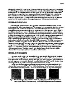
Experimental: Thin Si0 2 films of 20 and 30 nm thickness were thermally grown on n-type (100) Si wafers. Subsequently the layers
Data Loading...