Raman Vibrational Study of Pulsed Laser Annealing of Implanted GaAs
- PDF / 297,688 Bytes
- 5 Pages / 420.48 x 639 pts Page_size
- 79 Downloads / 403 Views
RAMAN VIBRATIONAL STUDY OF PULSED LASER ANNEALING OF IMPLANTED GaAs J. SAPRIEL and Y.I. HJISSIM Centre National d'Etudes des T6l6communications, 196 rue de Paris, 92220 Bagneux - (FRANCE)
Laboratoire de Bagneux,
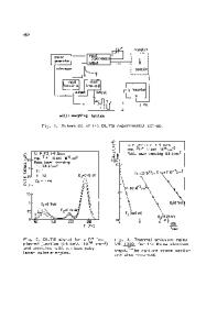
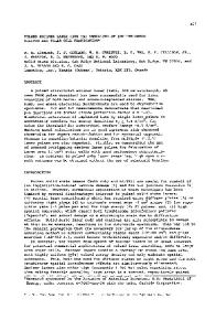
ABSTRACT The lattice reconstruction produced by a pulsed laser irradiation in heavily damaqed GaAs layers is studied. Spatially resolved Raman measurements are used to characterize the crystalline auality after the annealing cycle produced by a 0-switched Ruby laser or by a picosecond pulsed Nd-YAG laser. The continuous evolution in the Raman spectra is us6d to follow the crystal recovery as a function of the irradiation parameters. ItNTRODUCTION Compound Semiconductors, and in particular GaAs, have from the start been potential candidates for the application of the beam annealinq technology. Pulsed beams have been used successfully to reconstruct ion-implanted damaged layers [1] with partial electrical activation. Pulsed lasers have been used in this study to reconstruct heavily damaged layers in GaAs. Two kinds of laser beams were used to perform the annealing : a nanosecond Qswitched Ruby laser (25 nsec) and a picosecond mode-locked Nd-YAG laser (30 psec) at 1.06 ýim wavelength. After irradiation the samples were characterized by means of Raman scattering by lattice vibrations (phonons). Raman scattering is a versatile and non-destructive tool to analyse the lattice reconstruction. In particular it has been possible to follow continuously the evolution of the Raman spectra for different recrystallization stages. I - ANNEALING OF GaAs AS A FUNCTION OF THE ENERGY DENSITY OF A NANOSECOND PULSED RUBY LASER Two different Indium ion implantations have been superposed in order to 15 2 obtain a uniform distribution of defects, one at 330Kev (dose 3x10 cm- ) 15 2 and the other at 170Kev (dose 1.5x10 cm- ). Such experimental conditions allowed the formation of an amorphous GaAs layer of thickness (1O000), larger than the penetration depth of the incident light of the argon-ion laser used to perform the Raman measurements which are thus unaffected by the (001) oriented crystalline substrate. Several pulses carrying a uniform energy density W in the range O.1J/cm2 - 1J/cm2 have been used. We have then investigated the annealing effect corresponding to the different values of W by means of a conventional Raman experimental set up (2] using a T800 Coderg triple monochromator and an Ar+ laser on the 5145 and 4880A exciting lines. About 300mW of the laser beam were directed on the samples at the Brewster incidence to maximize the transmitted power. The samples were investigated under vacuum to suppress the low-frequency Raman lines of the air. The scattered light intensity I (N) of an amorphous material is given 3by I (W) =cbn(wT) + 1] gb(w) where n(wT) is the Bose-Einstein b
distribution at temperature T for first-order Stokes scattering at energy shift w and g (w) represents the vibrational density of states in band b
Mat. Res.Soc.Symp. Proc. Vol. 23 (1984) 0Elsevier Science Publishing Co., Inc.
714
Cb is the c
Data Loading...