Comparison of Pulsed Laser and Furnace Annealing of Nitrogen Implanted Silicon
- PDF / 799,018 Bytes
- 6 Pages / 417.6 x 639 pts Page_size
- 62 Downloads / 324 Views
COMPARISON OF PULSED LASER AND FURNACE ANNEALING OF NITROGEN IMPLANTED SILICON T. P. SMITH, III and P. J. STILES Physics Department, Brown University, W. M. AUGUSTYNIAK, Bell Laboratories,
Providence,
RI 02912
W. L. BROWN, and D. C. JACOBSON Murray Hill, NJ 07974
R. A. KANT Naval Research Laboratory,
Washington,
DC 20375
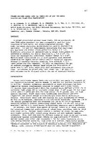
ABSTRACT Formation of buried insulating layers and redistribution of impurities during annealing are important processes in new semiconductor device technologies. We have studied pulsed ruby laser and furnace annealing of high 17 2 dose (D>10 N/cm ) 50 KeV nitrogen implanted silicon. Using He Backscattering and channeling, X-ray diffraction, transmission electron microscopy, and infrared transmission spectroscopy, we have compared liquid and solid phase regrowth, diffusion, impurity segregation and nitride formation. As has been previously reported, during furnace annealing at or above 1200C nitrogen redistributes and forms a polycrystalline silicon nitride (Si3N4 ) layer. [1-4] In contrast, pulsed laser annealing produces a buried amorphous silicon nitride layer filled with voids or bubbles below a layer of polycrystalline silicon. INTRODUCTION Furnace annealing on high dose nitrogen implanted silicon has been studied by several workers, [1-4], but little work has been done using pulsed laser annealing. [5,6] We have found striking differences between furnace and pulsed laser annealing of this material. Furnace annealing is rather insensitive to changes in implant dose, D, while resolidification following pulsed laser melting of nitrogen implanted silicon is highly dose dependent. EXPERIMENTAL N-type (111) silicon wafers were implanted with 50 KeV N+ ions or 100 2 KeV N2 + ions at room temperature to doses of 1.4 to 6.6 x 10¹⁷ N/cm . The samples were then furnace annealed at 1200C for 2 hours or irradiated with 30 ns ruby (X=694nm) laser pulses with energy densities between 0,5 and 2.6 2 J/cm . The laser spot size was 5mm in diameter and uniform to ±5 percent. 2.0 MeV helium ion Rutherford backscattering (RBS) and channeling were performed at scattering angles of 180 and 105 degrees. 105 degrees was chosen because it gave the maximum depth resolution (approximately 2.8 times that at 180 degrees) without moving the nitrogen peak too close to the dip in the silicon spectra caused by reduced silicon scattering due to the presence of a high nitrogen concentration (see figure 1). X-ray diffraction was performed with a Read camera. Infrared transmission spectra were compared by 1 using the silicon absorption band at 610 cmas an internal standard. 2 Current-voltage characteristics were measured by evaporating 1.8 x 10⁻³ cm aluminum dots on the surface and using the aluminum as a mask to etch mesas and as electrical contacts.
Hat. Res. Soc. Symp. Proc. Vol. 23 (1984) @ Elsevier Science Publishing Co.,
Inc.
454
--.-
(111) As Implanted .(R ) 2 .0 Jlcm z 2 (11) 2.0 J/cm 111)1200C
"(-
1.0
1.2
1.3
1.4
Energy (MeV) Figure 1. 105 degree RBS spectra for silicon implanted with 100 KeV N2 + to 2
Data Loading...