Microstructural and Electrical Characterization of Misfit Dislocations at the InAs/GaP Heterointerface
- PDF / 1,023,240 Bytes
- 6 Pages / 414.72 x 648 pts Page_size
- 92 Downloads / 300 Views
orthogonal arrays of 90' edge dislocations [2]. 900 dislocations are known to relieve strain more efficiently than 600 dislocations and hence their presence is favored at a high lattice mismatch. InAs is a narrow gap semiconductor with very high electron mobility. It shows potential for devices such as Infra-Red emitters and detectors, low temperature transistors, thermophotovoltaics, etc.. We have investigated the direct growth of InAs on (001) GaP. This system has the largest lattice mismatch among the III-arsenides and the III-phosphides: - 11%. In addition, the large band offsets between InAs (band gap, Eg=0. 36 eV) and GaP (Eg= 2 .2 6 eV) result in interesting heterojunction properties. Heterojunction InAs/GaP diodes have shown near ideal forward and reverse bias characteristics and reasonable breakdown voltages [3]. The InAs epilayer was found to be 80% relaxed and lattice matched to In 0. 8A10. 2As and In 0 .8Gao. 2As [4]. EXPERIMENT InAs was grown on (001) GaP by Solid Source Molecular Beam Epitaxy (SSMBE) using a Varian GEN-II MBE system. A I ) nm GaP buffer layer was grown followed by the growth of a twenty period superlattiue consisting of 5 nm alternating layers of GaP and AlP in order to prevent the out diffusion of sulfur from the substrate. Finally a 200 nm buffer layer of p-GaP 3 (_1016 cm" ) was grown at 600'C. An undoped InAs epilayer was grown at 350 0 C at a growth 63 Mat. Res. Soc. Symp. Proc. Vol. 500 ©1998 Materials Research Society
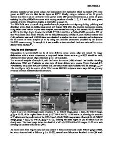
rate of 0.7 monolayers per second. The first few monolayers were grown under a low Vill[ beam flux ratio to promote a smoother interface. Finally, a cap layer of undoped In o.s AI0.2As was grown above the InAs layer. The cap layer is lattice matched to the 80% relaxed InAs, and has a wider band gap. Samples with varying thickness of InAs in the range of 5 nm to 30 run were grown in this manner. A schematic sketch of the multilayer structure grown is shown in Figure 1. In 0 .sAi 0 . 2 As - undoped
5 nm
80% relaxed InAs - undoped
5 - 30 nm
S....
p- - GaP (-1 X
,10U)
I
200 nm
n AIGaP/GaP Superlattice (-1 X 101)
n - GaP Sub (-2 X 10¹⁸)
Figure 1 : Schematic illustration of the multilayer structure grown by MBE
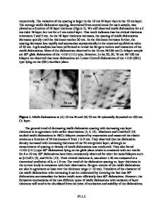
Cross-sectional and plan view TEM studies were performed using a JEOL 2000 FX microscope with a beam energy of 200 keV. Despite the high lattice mismatch, a perfect epitaxial relationship between the [nAs and GaP was observed in all cases, as revealed by electron diffraction patterns. Figure 2 shows a HRTEM micrograph of the InAs/GaP heterointerface. A regularly spaced array (spacing - 4 nm) of predominantly 900 misfit dislocations oriented along is clearly visible at the interface. The regions of the interface between the dislocations appears to be atomically smooth and free of distortions. Thus, the interface structure consists of two orthogonal arrays of sessile 900 edge dislocations lying on the (001) plane with mutually perpendicular 1/2 Burgers vectors.
Figure 2: HRTEM micrograph of InAs/GaP heterostructure displaying regularly spaced 900 mis
Data Loading...