Silicide Formation at HfO 2 /Si and ZrO 2 /Si Interfaces Induced by Ar + Ion Bombardment
- PDF / 288,854 Bytes
- 6 Pages / 595 x 842 pts (A4) Page_size
- 115 Downloads / 416 Views
E3.25.1
Silicide Formation at HfO2/Si and ZrO2/Si Interfaces Induced by Ar+ Ion Bombardment Yu. Lebedinskii, A. Zenkevich, D. Filatov1, D. Antonov1, J. Gushina1, G. Maximov1 Moscow Engineering Physics Institute, 115409 Moscow, Russia 1 University of Nizhny Novgorod, 603950 Nizhny Novgorod, Russia ABSTRACT The effect of ion bombardment with Ar+ at the energy E=2.5 keV on HfO2/Si and ZrO2/Si interfaces has been investigated in situ with XPS by growing thin metal oxide layers and further ion etching them. It is shown that a silicide layer ~2 nm in thickness is forming, and Ar+ ion beam affects MeO2/Si (Me=Hf, Zr) interface at thickness ≤3 nm. Ex situ AFM/STM corroborates the formation of silicide layer at metal oxide/silicon interface. INTRODUCTION The area of advanced gate dielectrics has got much attention recently due to the prospect of replacing silicon dioxide as the gate dielectric material for standard CMOS technology [1-2]. High-k metal oxides have been considered as alternate materials to provide substantially (physically) thicker dielectric layer for reduced leakage and increased gate capacitance. Among those oxides, HfO2 and ZrO2 are considered to be the most promising candidates. The stability of the interface between high-k dielectric layer and Si channel, particular upon thermal annealing of the stack, is of primary importance. Recently, the metal silicide formation has been observed for HfO2 /Si and ZrO2 /Si systems as a result of thermal treatment [3,4,5]. Ar+ ion bombardment is used widely for etching of thin films in surface analysis techniques (XPS, AES, SIMS, etc.) for the composition depth profiling (as well as for ion milling of Zr4+
Zr 3d Zr0
interface
bulk surface 190.0 187.5 185.0 182.5 180.0 177.5
Binding energy, eV
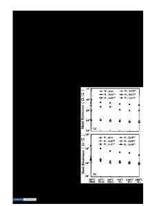
Figure 1. Typical XP spectra recorded during Ar+ beam ion etching of ALD grown ZrO2 layer on Si. samples in TEM). It is especially beneficial to approach the interface of a thick oxide layer on Si to be able to probe it with surface sensitive techniques, in particular, x-ray photoelectron spectroscopy (XPS). At the same time, it is known that ion bombardment may affect both
E3.25.2
elementary and chemical compositions of the subsurface layer within ion range, particularly, the formation of silicides at metal/Si interface [6,7, 8]. We normally observe silicides at the interface during depth profiling of HfO2 and ZrO2 layers grown on Si. In figure 1 the evolution of x-ray photoelectron spectra during routine depth profiling of ALD grown ZrO2 layer on Si, employing Ar+ ion beam (E=2.5 keV) is shown. While no visible chemical effect is seen etching the “bulk” of oxide layer 20 nm thick, the lower BE component in Zr3d line corresponding to unoxidized Zr (or silicide) is emerging clearly once the etching front has approached the ZrO2/Si interface. However, the full set of spectra seems inconsistent taking into account the free path of escaping electrons, since the silicide “interface” layer should have manifested itself much earlier. In the present work, we demonstrate that the
Data Loading...