Morphologies and Related Electronic Properties of Carbon Nanotubes
- PDF / 354,649 Bytes
- 12 Pages / 612 x 792 pts (letter) Page_size
- 80 Downloads / 278 Views
MATERIALS RESEARCH
Welcome
Comments
Help
Morphologies and related electronic properties of carbon nanotubes J-C. Charlier Unit´e de Physico-Chimie et de Physique des Mat´eriaux, Universit´e Catholique de Louvain, 1 Place Croix du Sud, B-1348 Louvain-la-Neuve, Belgium (Received 29 January 1998; accepted 3 May 1998)
The electronic structures of different morphologies of carbon nanotubes are investigated within either tight-binding or ab initio frameworks. After a brief description of the electronic properties of the “perfect” rolled-up graphene sheet, nanotubes containing pentagon-heptagon pairs, tips (hemispherical caps), sp3 -like lines responsible for polygonization, multishell and solid-state packings (bundles) are studied in order to point out the influence of such defects on the electronic states of the “perfect” cylinders. Most of the time, a structural optimization was performed on the atomic topology, prior to the calculation of the electronic properties. Connections with experimental facts are indicated as frequently as possible.
I. INTRODUCTION
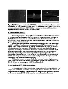
Carbon nanotubes have their origin at the crossroad of traditional carbon fibers and the novel fullerenes, and thus constitute the link between mechanical reinforcements in composites and molecular wires that could lead to ideal electrical connectors in future technology.1 Microscopically, a nanotube consists of one (singlewall2,3 ) or more (multiwall4 ) coaxial cylindrical rolledup graphene sheets, separated by approximately the interlayer distance of graphite (0.34 nm). The size distribution is 0.8–3 nm diameter for single-wall nanotubes and 2–30 nm diameter for multiwall nanotubes, both being generally microns in length, extremely stiff with very high axial strength,5 and also often observed in bundles.6,7 The small diameter of nanotubes makes it easy to see why they can be thought of as quantum wires and therefore why the interest in their electronic properties. With the notion of helicity introduced by Iijima,4 the electronic properties of carbon nanotubes have been studied extensively in many theoretical works.8–13 All these calculations pointed to one important conclusion: the electronic properties of the nanotube would vary in a periodic way between metallic and semiconductor as a function of both the diameter and the helicity. Using Fig. 1(a), the chirality and the tube diameter of any graphene tubule can be specified in terms of the chiral vector Ch na1 1 ma2 which connects two crystallographically equivalent sites on a 2D graphene sheet.9 The construction in Fig. 1(a) shows the chiral angle u with respect to the zigzag direction su 0d and the unit vectors a1 and a2 of the hexagonal honeycomb lattice. The armchair tube [Fig. 1(a)] corresponds to a1 and a2 of the hexagonal honeycomb lattice. The armchair tube [Fig. 1(a)] corresponds to u 30± on this 2368
J. Mater. Res., Vol. 13, No. 9, Sep 1998
construction. An ensemble of possible vectors specified by pairs of integers sn, md denoting the vector Ch na1 1 ma2 is given in Fig. 1(b). In the (
Data Loading...