Morphology of Low Temperature Carbon Films Prepared by VHF CVD: Correlation with Field Emission
- PDF / 899,083 Bytes
- 6 Pages / 414.72 x 648 pts Page_size
- 99 Downloads / 335 Views
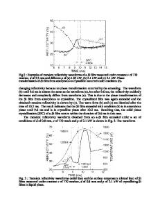
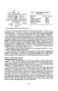
ABSTRACT The effect of deposition parameters and substrate on the morphology of carbon films prepared in VHF plasma at low temperature has been studied by Atomic Force Microscopy. Carbon films demonstrating superior emission characteristics were the smoothest, but not all of the smoothest films demonstrated good emission. Significant influence of pre-growth treatment of the substrate surface on the emission characteristics of the films was found. INTRODUCTION Electron field emission (FE) from various carbon materials (natural diamond, CVD diamond, diamond-like-carbon films, amorphous carbon etc.) is widely studied as promising for microelectronic field emission devices. FE observations under relatively low electric fields (in the range of 3-40 V/tm) have been reported [1-4]. Negative Electron Affinity (NEA) observed in natural diamond from certain surfaces terminated with H [5, 6] or Cs [7] was proposed for explanation for the high FE. Polymeric wide band gap a-C:H films, as suggested from the results of photoelectron yield measurements, has also low electron affinity [8]. However, recent results on polycrystalline diamond gave evidence that electrons are emitted from a graphite like phase of diamond at grain boundaries [9]. Rather effective emission from non-diamond carbon (NDC) films and improvement of emission from silicon tips with NDC coating were found [10]. There are also other arguments in favor of NEA playing some role, but this can not be the only mechanism of field emission. As observed by many investigators, electrons are emitted nonuniformly from the surface. Groening et al. [11] observed the generation of emitting spots due to vacuum arc discharge preceding FE. From rough or inhomogeneous materials FE started at lower field of 3 V/l.m than from smooth surfaces [12-14]. Correlation of morphology of NDC coating on silicon tips with electron emission was observed by Kosarev et al. [10]. From studying field emitted electron energy distribution, Kuetttel et al. [15] obtained reasonable values of both work function (5 eV) and field enhancement coefficient 13=450. But the physical reason of such significant field enhancement is still unclear. One possibility is film surface morphology. This work is devoted to AFM study of morphology of carbon films prepared by Very High Frequency (VHF) CVD in a capacitance coupled discharge at relatively low substrate temperatures (T,
Data Loading...