Multi-Scale Simulations of Silicon Etching by Halides: Effects of Surface Reaction Rates.
- PDF / 1,012,697 Bytes
- 6 Pages / 612 x 792 pts (letter) Page_size
- 31 Downloads / 290 Views
Multi-Scale Simulations of Silicon Etching by Halides: Effects of Surface Reaction Rates. Matthias Kratzer, Werner Steinhögl, Alfred Kersch, Tanja Sachse, Volker Höink Infineon Technologies AG, Memory Products, 81541 München, Germany
ABSTRACT We investigate the reactive ion etching of amorphous silicon by halides using a hierarchy of models on different time and length scales. The feature evolution is modeled using a twodimensional cell based Monte-Carlo feature scale simulator. The fluxes, the energy distributions, and the angular distributions of the wafer-incident particles are provided by a hybrid plasma sheath simulator. The relevant surface reaction rates are calculated by a molecular dynamics simulator using a Stillinger-Weber representation of the interatomic potential. Our investigations show that the surface reaction rates are strongly determined by the particular surface morphology, which, in turn, is strongly influenced by the kinetic properties of the impinging particles. Thus, we link the molecular dynamics simulator into the model as a whole. As results, we present calculations for the etching of amorphous silicon by fluorine, chlorine, and bromine. A Stillinger-Weber representation of the bromine and the silicon-bromine potential which was not yet available in literature is additionally developed. We discuss the different morphologies of halogenated silicon surfaces as a consequence of the energy distribution and the angular distribution of the impinging particles. Comparisons of the sputter yield functions of bare amorphous silicon surfaces and corresponding halogenated surfaces exhibit considerable differences, qualitative as well as quantitative.
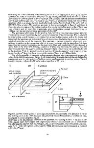
INTRODUCTION Simulation methods are used in microelectronics industry for the understanding and the optimization of complex physical processes. A typical example is the investigation of surface patterning processes. Many of them are plasma based, i.e. plasma etching (PE), reactive ion etching (RIE), plasma-assisted chemical vapor deposition (PECVD), or ionized physical vapor deposition (IPVD) [1-3]. For the simulation of such a process, it is necessary to describe the plasma conditions as well as the evolution of the features on the wafer being processed. Linking these different length scales together in one unified model, is one of the central challenges of current simulators. As shown in figure 1, the details of the etching yield functions have a crucial impact on the feature evolution. Nevertheless, many feature scale models still rely on largely empirical expressions of surface reaction rates [4,5]. More recent models use etching yield functions which have been calculated separately by molecular dynamics simulations [6-8]. We investigate the reactive ion etching of silicon by halides which is widely used in VLSI manufacturing. The process gas (typically NF3, Cl2, or HBr) is dissociated into radicals using some kind of rf driven discharge. These radicals form a chemisorbed layer (SiFx, SiClx, and SiBrx, respectively) of several monolayers thickness o
Data Loading...