New Pairs of Inks and Papers for Photolithography, Microcontact Printing, and Scanning Probe Nanolithography
- PDF / 1,291,709 Bytes
- 6 Pages / 612 x 792 pts (letter) Page_size
- 60 Downloads / 340 Views
F3.2.1
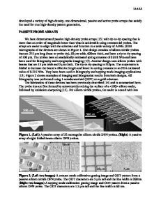
New Pairs of Inks and Papers for Photolithography, Microcontact Printing, and Scanning Probe Nanolithography Lon A. Porter, Jr., Hee Cheul Choi, J. M. Schmeltzer, Alexander E. Ribbe, and Jillian M. Buriak Department of Chemistry, 1393 Brown Laboratories, Purdue University, West Lafayette, IN 47907-1393, U.S.A. ABSTRACT Currently, there is considerable interest in producing patterned metallic structures with reduced dimensions for use in technologies such as ultra large scale integration (ULSI) device fabrication, nanoelectromechanical systems (NEMS), and arrayed nanosensors, without sacrificing throughput or cost effectiveness. Research in our laboratory has focused on the preparation of precious metal thin films on semiconductor substrates via electroless deposition. This method provides for the facile interfacing of metal nanoparticles with a group (IV) and III-IV compound semiconductor surfaces. Morphologically complex films composed of gold, platinum, and palladium nanoparticles have been prepared as a result of the immersion of germanium and gallium arsenide substrates into dilute, aqueous solutions of tetrachloraurate (III), tetrachloroplatinate (II), and tetrachloropalladate (II), respectively. Continuous metallic films form spontaneously under ambient conditions, in the absence of a fluoride source or an externally applied current. This facile electroless deposition methodology provides an alternative to complex and expensive vacuum methods of metallization, yet allows for the preparation of both thin and thick nanostructured films with control over surface morphology and deposition rate. Furthermore, precious metal films prepared in this way exhibit excellent adhesion to the underlying semiconductor substrate. The resultant films were characterized utilizing scanning electron microscopy (SEM), X-ray photoelectron spectroscopy (XPS), and scanning probe microscopy (SPM). In order to apply this novel metallization method toward the development of useful technologies, patterning utilizing photolithography, microcontact printing (µCP), and scanning probe nanolithography (SPN) has been demonstrated. INTRODUCTION Patterning metallic structures with micro- and nanometer resolution for both fundamental investigations and technological applications has recently attracted considerable interest. Developments toward this end, such as dip-pen nanolithography (DPN) [1] and micro-contact printing (µ-CP) [2], employ a liquid-phase “ink” to pattern a solid “paper” substrate. These are relatively straightforward methods to execute since they operate in air, using easily accessible equipment and simple procedures. Herein, we report the patterning of new pairs of metallic or semiconducting papers with inks of aqueous noble metal salts, chosen on the basis of mixed potential arguments [3], through photolithography, µ-CP, and DPN [4]. The resulting nanoparticle films deposited from these inks demonstrate complex morphological architectures [3], which are of importance
F3.2.2
for the interfacing of nanoparticles with me
Data Loading...