Ni-Induced Selective Nucleation and Solid Phase Epitaxy of Large-Grained Poly-Si on Glass
- PDF / 610,040 Bytes
- 10 Pages / 612 x 792 pts (letter) Page_size
- 59 Downloads / 279 Views
NI-INDUCED SELECTIVE NUCLEATION AND SOLID PHASE EPITAXY OF LARGE-GRAINED POLY-SI ON GLASS Rosaria A. Puglisi1, Hiroshi Tanabe, Claudine M. Chen, Harry A. Atwater, Emanuele Rimini2 California Institute of Technology, T. J. Watson Laboratory of Applied Physics, MS128-95, Pasadena, CA USA 1 Temporary fellowship at ST-Microelectronics, Str.le Primosole 50, 95121 Catania, Italy 2 Universita' di Catania, Dipartimento di Fisica, and Unità INFM, Corso Italia 57, 95100 Catania, Italy.
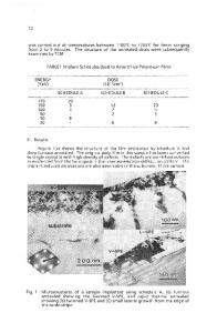
ABSTRACT We investigated the formation of large-grain polycrystalline silicon films on glass substrates for application in low-cost thin film crystalline silicon solar cells. Since use of glass substrates constrains process temperatures, our approach to form large-grain polycrystalline silicon templates is selective nucleation and solid phase epitaxy (SNSPE). In this process, selective crystallization of an initially amorphous silicon film, at lithographically predetermined sites, enables grain sizes larger than those observed via random crystallization. Selective heterogeneous nucleation centers were created on undoped, 75 nm thick, amorphous silicon films, by masked implantation of Ni islands, followed by annealing at temperatures below 600 °C. At this temperature, the Ni precipitates into NiSi2 particles that catalyze the transition from the amorphous to the crystalline Si phase. Seeded crystallization begins at the metal islands and continues via lateral solid phase epitaxy (SPE), thus obtaining crystallized regions of several tens of square microns in one hour. We have studied the dependence of the crystallization rate on the Ni-implanted dose in the seed, in the 5x10¹⁵/cm3 - 1016/cm3 range. The large grained polycrystalline Si films were then used as a substrate for molecular beam epitaxy (MBE) depositions of 1 µm thick Si layers. Transmission electron microscopy (TEM) analysis showed a strong correlation between the substrate morphology and the deposited layer. The layer presented a large grain morphology, with sizes of about 4 µm.
INTRODUCTION 1 Permanent address: INFM and Università di Catania Physics Dept. Corso Italia 57 95100 Catania Italy email: [email protected]
O8.1.1
Polycrystalline silicon (poly-Si) thin films on glass are currently attracting a great deal of attention for use in solar cells. Crystalline Si solar cells are well-known for their high efficiencies [1], while glass is one of the cheapest substrate materials and allows one to make very efficient light trapping [2]. Yet, the limited thermal stability of glass and its amorphous nature led to the development of a great variety of techniques to deposit and crystallize [3] device-grade crystalline Si films or to transfer monocrystalline Si films onto glass [4 to 8]. Commercial glass limits the maximum processing temperature of Si films to 600°C. Also, in order to collect most of the generated charge carriers within a Si film, an effective diffusion length of the minority carrier in the polycrystalline Si film larger than the film thickness has to be achiev
Data Loading...