TEM Characterization of Solid-Phase Epitaxy in Amorphized Polysilicon
- PDF / 2,645,668 Bytes
- 6 Pages / 417.6 x 639 pts Page_size
- 3 Downloads / 320 Views
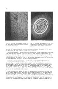
TEM CHARACTERIZATION OF SOLID-PHASE EPITAXY INAMORPHIZED POLYSILICON P.-H. Chang* and R. Sundaresan** "*CentralResearch Laboratories, MS 147, Texas Instruments Incorporated, Dallas, TX 75265 "**SemiconductorProcess and Design Center, MS 944, Texas Instruments Incorporated, Dallas,TX 75265. ABSTRACT Solid Phase Epitaxy (SPE) of amorphous silicon thin films can be employed to build novel device structures for VLSI applications. One way of achieving SPE is to use a room temperature silicon implant to amorphize a polysilicon layer followed by a thermal treatment to promote epitaxial growth. Both vertical SPE, in which the epitaxial film is grown directly on silicon substrate, and lateral SPE, in which the epitaxial growth is extended over a thin layer of oxide using the vertical SPE region as a seed, have been realized using this approach. This paper presents results obtained by cross-sectional TEM analysis of the epitaxial films, with particular emphasis on the effects of implant schedule and annealing conditions on the epitaxial regrowth. I. INTRODUCTION Solid phase epitaxial growth of amorphous Si (a-Si) films is a promising technique to realize some novel CMOS devices for silicon-on-insulator (SOl) and three dimensional integration[1-3]. In this method, amorphous Si layer on crystalline Si substrate is recrystallized epitaxially first (vertical solid phase epitaxy or V-SPE). The V-SPE region is then used as a seed to grow laterally into the amorphous film over a thin layer of oxide. The latter process is generally termed as lateral solid phase epitaxy (L-SPE). So far, experimental results on SPE growth of three types of a-Si films have been reported: (a) ultra high vacuum evaporated a-Si[1, (b) a-Si film deposited by a clean-CVD process[2] and (c) a-Si film formed by high dose silicon implant of LPCVD polysilicon film[3]. Of these methods the first two require an in situ cleaning of the substrate surface prior to film deposition while the last approach can be carried out on chemically cleaned substrate surface. This paper investigates the materials characteristics of the SPE films obtained by method (c). Instead of implanting Si at the liquid nitrogen temperature as others have done previously[3], room temperature Si implant was used to amorphize the polysilicon film in an effort to make this process practicable. The purpose of this investigation is to study the effects of implant condition and subsequent annealing on the quality of the SPE films. II. EXPERIMENT Silicon slices were thermally oxidized to form a 50 nm thick oxide. The oxide was patterned and etched to give alternating regions of silicon and oxide. After cleaning and rinsing in a 10% HF solution the slices were loaded into a LPCVD furnace and a 150 nm thick polysilicon film was deposited. The poly film was subsequently amorphized by a room temperature silicon implant using four different implant schedules listed in Table I. After the implant the slices were either furnace annealed or rapid thermal annealed. The furnace anneal was performed for 5 days
Data Loading...