On-Chip Testing of Mechanical Properties of MEMS Devices
- PDF / 408,217 Bytes
- 2 Pages / 612 x 792 pts (letter) Page_size
- 82 Downloads / 417 Views
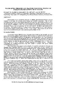
is anisotropic and varies from 0.80 to 0.95 MPa m1/2. MEMS, like microelectronics, use chemical vapor deposition to deposit polysilicon films. A variety of microstructures can be produced, depending on the deposition parameters and postdeposition heat treatments.5 Micron-scale specimens are fabricated, a sharp pre-crack is produced by indentation, and the specimen is loaded using an integrated MEMS electrostatic actuator.6 The actual indent takes place on the substrate, away from the specimen, and the crack propagates into the specimen; in this way, the indentation-induced stresses and damage are avoided. The test structure is shown in Figure 1, and the results are presented in Table I. Note that single-crystal silicon specimens can also be fabricated using silicon-on-
On-Chip Testing
of Mechanical Properties of MEMS Devices
H. Kahn, A.H. Heuer, and R. Ballarini The field of microelectromechanical systems (MEMS) involves the interaction of the physical environment with electrical signals through the use of microbatchfabricated devices. MEMS is a growing technology, and commercial MEMS products are becoming commonplace. To optimize MEMS designs, materials properties must be thoroughly characterized and controlled. Device designers need to know the allowable strain limits as well as Young’s modulus, fracture strength and fracture toughness, thermal conductivity, and other key properties. For extrinsic materials properties, the statistical scatter is critical for determining reliability safety factors. While these values are generally known for bulk materials, it is not clear that they will be valid for materials with the characteristic microstructures and morphologies that result from MEMS processing. Also, as devices shrink, the ratios of surface area to volume become so large that surface properties, such as adhesion energy and friction, can control the performance (or failure) of MEMS devices. (For more on the tribology challenges of MEMS fabrication, see the article by de Boer and Mayer in this issue.) While it is obvious that the mechanical properties of MEMS materials must be measured to enhance device performance, it is equally true that the fabrication and operating techniques developed for MEMS can be exploited for performing basic materials-properties investigations. Previous efforts aimed at determining mechanical properties at micron-sized scales have been severely limited. Thin films on substrates can be studied using nanoindentation and microscratching with diamond indenters.1 Freestanding films can also be tested with specially designed equipment,2 although specimen handling is exceed300
ingly difficult. The ability of MEMS structures to be reliably released from their substrates, actuated, and then to move in a controlled fashion permits a tremendous range of experiments; essentially, any measurement taken at the macroscale can be analogously repeated at the microscale. In addition, the batch fabrication inherent to MEMS processing creates a multitude of identical specimens that can generate data
Data Loading...