Optical Characterization of Mg- and Si-Implanted GaN
- PDF / 206,070 Bytes
- 6 Pages / 612 x 792 pts (letter) Page_size
- 25 Downloads / 315 Views
Optical Characterization of Mg- and Si-Implanted GaN James A. Fellows,1 Yung Kee Yeo,1 Robert L. Hengehold,1 and Leonid Krasnobaev 2 Air Force Institute of Technology, Wright-Patterson AFB, OH 45433, U.S.A 2 Implant Sciences Corp, Wakefield, MA 01880-1246, U.S.A 1
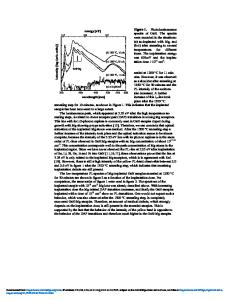
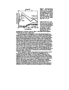
ABSTRACT The optical and electrical properties of Mg- and Si-implanted GaN were investigated using photoluminescence, cathodoluminescence, and Hall-effect measurements. Implantation of Mg, Si, Mg+Si, Mg+O, Mg+C, and Mg+P was made into undoped semi-insulating MBE-grown GaN at energies from 125 to 260 keV at room temperature and 800 oC with doses of 1x10¹⁴ to 5x1015 cm-2. The samples were capped with AlN and annealed at temperatures ranging from 1100 to 1300 oC for 9 s to 20 min. The dominant luminescence peak in all Mg-implanted and annealed GaN is a broad green luminescence (GL) band at 2.36 eV, which may be related to a deep donor-deep acceptor complex transition resulting from the Mg implant, residual implant damage, and/or native defects. The relative intensities of this GL band and secondary peaks from 2.75-3.28 eV vary as a function of implantation temperature, ion dose, species, and anneal temperature. All Mg single and dual implantation resulted in extremely resistive GaN layers, except Mg+Si, which resulted in weakly n-type GaN. However, the Si-implanted GaN produced an electrical activation efficiency as high as 73% after annealing at 1200 oC for 5 min. INTRODUCTION Wide band gap semiconductors such as GaN can provide many advantages and improvements over existing technology, particularly for specialized high-frequency, hightemperature, and high-power electronic devices, as well as blue to UV light emitting and detecting devices. In spite of these advantages, the fabrication of successful devices must still overcome several important problems. One of the problems associated with group-III nitride device technology is successfully doping impurities other than during growth. Ion implantation is one such doping technique, but the study of implantation doping of nitrides is still in its infancy, especially for p-type doping. Although this doping technique has many advantages including independent control of the doping level, the possibility of selective area doping, and the ability to fabricate planar devices and self aligned structures, one of the major problems is the need to anneal out the implantation damage and electrically activate the implanted ions. Although a significant amount of work has been done on acceptor ion-implanted GaN, only a limited amount of success has been reported in producing p-type conductive GaN via Mg [1,2], Ca [3], or Be [4] implantation which is not easily reproducible by other laboratories. In this paper, we report the results of both optical and electrical characterization studies of Mg- and Siimplanted GaN using Hall-effect, photoluminescence (PL), and cathodoluminescence (CL) measurement methods. EXPERIMENT The GaN layers were grown 2 µm thick by molecular beam epitaxy (MBE) on sapphire substrates with a 500 Å thick
Data Loading...


