Optical Properties of Si Nanocrystals Formed in SiO 2 by Ion Implantation
- PDF / 1,114,780 Bytes
- 6 Pages / 414.72 x 648 pts Page_size
- 93 Downloads / 414 Views
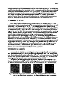
Fig. 1. Cross-section micrographs showing Si nanocrystals formed in SiO 2 when excess Si concentrations of (a) 5 x 10²'/cm 3 and (b) 2 x 10²²/cm 3 are annealed (1100 0C/l h/Ar + 4% H2). EXPERIMENTAL RESULTS Examples of Si nanocrystals formed in SiO 2 are shown in the micrographs of Fig. 1. Multiple energy implants were used to produce flat profiles (to -900 nm) with excess Si concentrations of 2 x 10²²/cm&and 5 x 10²¹/cm 3 . After annealing to cause precipitation, the average nanocrystal size is somewhat greater than 6 nm (with a few as large as 10 nm) in the sample with the higher concentration, whereas the average diameter is 3 nm in the sample with a concentration of 5 x 10 21/cm 3 . Consequently, the dose (or concentration) can be used to control the nanocrystal size.
"250000
100000 ........ ........ .......... ......... ........
S
t
200000 150000
0NOcO a0000 40000
1100000
I.
........ .... ............ ..........
.4..... .
. .... ............ ......... ,
ranneal
J
50000 0550
--------
S.......... t.................. ...... ,,... ..........
.j
I ...... ....
:H anneal
I. 600
650
700
750
01
800
5a0
850
600
650
700
750
eoo 850
900
Wavelength (nm)
Wavelength (nm)
Fig. 2. PL spectra from Si (400 keV, 1.5 x 10'/cme, RT) implanted SiOC in the as-implanted state and after annealing 0 at 9500 C and I I WC (I b/Ar + 4% H).
Fig. 3. PL spctra from Si (400 keV, 1.5 x 10¹⁷/cm 2) implanted SiO 2 after annealing for 1 h at 1 00°C in (a) Ar + H2 (b) pure Ar.
250
120
............. . ....... .............. -.................. 250000 .................. U a) 03
S
..........................
. .
S.....0. 00.
0
..
.........
...... ............... 5 ............. ............... 7I-
..i........ ......
C
Ci 12UUUU
*j 60
:310ý" ICM2(x20)
"•100000
C
50000
~
.1
700
800
0 .... S...
........
•...... .. .......... .............. ."...............
20
3 3333..3...L..L...
750
/c
S... 40
0 650
7
•x15°",
C
600
!.
8100
850
Wavelength (nm) 200
300
400
500
600
700
Wavelength (nm)
Fig. 4. Dose dependence of PL from Si (400 keV) implanted SiO 2 after annealing (1100 0C/1 h/Ar + H2).
Fig. 5. Optical transmission through Si (400 keV) implanted Si0 2 to the indicated dose after annealing (1 100°C/1 h/Ar + H2).
Figure 2 shows PL spectra (excited at 488 nm) from fused silica implanted by Si (400 keV, 1.5 x l0' 7 /cm 2, RT). The peak excess Si concentration is -5 x 10²¹/cm 3. In the as-implanted state, luminescence peaked at 650 nm is observed, which probably arises from defects introduced into the matrix during implantation.[2] Annealing at 950'C greatly reduces the defect luminescence. Annealing at 1100TC causes precipitation and Si nanocrystal formation, and after annealing an intense PL band peaked at -750 nm is observed. The intensity of this band is strongly dependent on the presence of H2 in the annealing environment as demonstrated in Fig. 3. Annealing in Ar + 4% H2 results in a very intense PL spectra, whereas annealing in pure argon gives rise to a PL intensity decr
Data Loading...