Synthesis and Properties of GaAs Nanocrystals in Sio 2 Formed by Ion Implantation
- PDF / 2,461,340 Bytes
- 6 Pages / 414.72 x 648 pts Page_size
- 8 Downloads / 352 Views
2
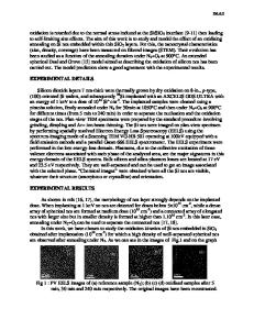
JANE G. ZHU,* C. W. WHITE, D. J. WALLIS,' J. D. BUDAI, AND S. P. WITHROW Oak Ridge National Laboratory, Solid State Division, Oak Ridge, TN 37831-6057 D. 0. HENDERSON, Fisk University, Physics Department, Nashville, TN 37208 ABSTRACT GaAs nanocrystals have been formed by the sequential ion implantation method. The sequence of Ga and As ion implantation (i.e., Ga + As or As + Ga) is found to affect the size distributions of GaAs nanocrystals significantly. The nanocrystal sizes are much bigger in the samples with Ga implanted first than those with As implanted first. This phenomenon is explained by the different diffusion behaviors of Ga and As species. Different precipitate regions have been observed in the samples implanted with Ga first and then As. Optical absorption measurements show that Ga particles have already formed in the as-implanted stage. INTRODUCTION Nanocrystals, exhibiting properties that are different from the bulk materials, are attracting considerable attention [1]. For semiconductor materials, the different band structures for nanocrystals lead to new electronic and optical properties. For optical applications, for example, visible luminescence has been observed from nanocrystal materials with an enlarged band gap due to quantum confinement effects [2,3]. Nonlinear optical properties can also be significantly enhanced for the nanocrystals compared to the bulk material [4]. Thus, investigations of semiconductor nanocrystals are necessary both scientifically and technologically. When the ion implantation technique is used to form GaAs nanocrystals, the whole process is entirely compatible with semiconductor technology [5-7]. For the formation of compound semiconductors, such as GaAs, where there is more than one element involved, there are material issues that need to be investigated. In this paper, we report our study on GaAs nanocrystals formed in SiO 2 by the ion implantation method. EXPERIMENTAL GaAs semiconductor nanocrystals were formed by ion implantation of Ga and As into a Si0 2 layer on (100) silicon, or a bulk silica glass substrate for optical absorption measurements, and subsequent thermal annealing. A typical Si0 2 layer was - 0.75 ýtm thick, formed by thermally oxidizing a (100) Si wafer. Equal doses of Ga (470 keV) and As (500 keV) were implanted at room temperature. The implant energies were chosen to overlap the peak concentrations in the middle of the oxide layer. Samples were annealed isochronally for I h under Ar + 4%H2 ambient at atmospheric pressure. The annealing temperatures varied from 800°C to 1000*C. The nanocrystalline structures were investigated by transmission electron microscopy (TEM). All the TEM specimens were prepared in cross sections, since the concentration distribution from ion implantation is a function of depth. Depth profiles of implanted Ga + As ions were examined by Rutherford backscattering spectrometry (RBS) using 2.3 MeV He 2 + beam. Selected samples were also examined by scanning transmission electron microscopy (STEM) with parallel electron ener
Data Loading...