OUM Nonvolatile Semiconductor Memory Technology Overview
- PDF / 259,122 Bytes
- 9 Pages / 612 x 792 pts (letter) Page_size
- 10 Downloads / 382 Views
0918-H05-01-G06-01
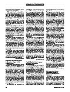
OUM Nonvolatile Semiconductor Memory Technology Overview Stephen J. Hudgens Ovonyx Technologies, Inc., 1030 East El Camino Real, #276, Sunnyvale, CA, 94807 ABSTRACT OUMTM (Ovonic Unified Memory), also called PCRAM (phase-change RAM) or CRAM (chalcogenide RAM), is a nonvolatile semiconductor memory technology being developed by Ovonyx, Inc. in a number of industrial joint development programs. OUM technology is based on an electrically initiated reversible amorphous to crystalline phasechange process in multi-component chalcogenide alloy materials similar to those used in rewriteable optical disks. Fundamental processes in phase-change memory devices, manufacturing technology, and progress towards commercialization of the technology will be reviewed. MEMORY CELL OPERATION Phase-Change Phase-change memory exploits an electrically-initiated, reversible phase-change between a glassy and a microcrystalline structural state in certain chalcogenide alloy semiconductors, most often Ge2Sb2Te5 (GST225) and related materials. The ordered or disordered structural state is achieved during device programming by controlling the temperature in the active volume of phase-change material and its time rate of change as shown in Fig. 1. The RESET state is achieved by applying a short (~ 10 ns) current pulse sufficient to melt a volume of the GST alloy adjacent to the bottom electrical contact. Rapid cooling of the molten volume after termination of the programming pulse results in formation of the metastable amorphous phase. The molten volume will become amorphous if the cooling rate is faster than the characteristic crystallization time, shown as t1 in the figure. The microcrystalline SET state is achieved either by applying a lower constant-amplitude current pulse for a time longer than t1 (SET pulse a.) or by using a SET-sweep pulse (SET pulse b.) which can be identical to a RESET pulse in its leading edge, but which ramps smoothly down with a fall time longer than t1 in its falling edge. Once the current in the SET-sweep has fallen to a value where no significant additional crystal growth will occur, it is terminated as shown in the figure. The SET-sweep programming technique [1] is used to achieve a more reliable, low resistance SET state in both individual memory cells and in device arrays since, during the sweep, all portions of the active volume in the GST can be subjected to an optimal crystallization temperature for an optimal duration to achieve crystallization. This technique can compensate both for temperature gradients within individual cells and for variations among all of the bits in an array [2].
Figure 1. Schematic temperature-time relationship during SET and RESET programming of phase-change memory. Ta and Tx are the amorphization and crystallization temperatures, respectively. A number of alloys other than GST225 have been investigated for use in phasechange random access memory, principally with the goals of reducing programming current, increasing crystallization temperature to improve data r
Data Loading...