Oxide Charging Effects by PH 3 /He Ion Shower Doping
- PDF / 141,317 Bytes
- 5 Pages / 612 x 792 pts (letter) Page_size
- 18 Downloads / 336 Views
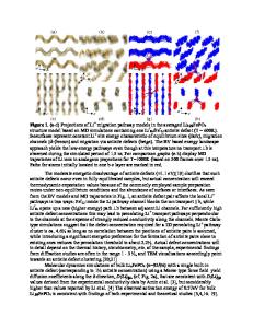
Oxide Charging Effects by PH3/He Ion Shower Doping Cheon-Hong Kim, Juhn-Suk Yoo, Kee-Chan Park and Min-Koo Han School of Electrical Engineering, Seoul National University, San 56-1 Shinlim-dong, Kwanak-gu, Seoul 151-742, Korea ABSTRACT We report the oxide charging effects on metal oxide semiconductor (MOS) structure caused by PH3/He ion shower doping. The parallel negative shift of flat-band voltage occurred for the ion-doped PETEOS samples even after thermal annealing. When the ion dose was higher, this shift was larger. These results show that a considerable amount of positive charges were induced inside the oxide films after PH3/He ion shower doping process. For the same ion dose, the flat-band voltage shift is larger when the thickness of PETEOS is thicker. When the ion dose was 1.5×1017cm-2 and the thickness of PETEOS was 80nm, the shift of flat-band voltage was larger than –7V. We can conclude that PH3/He ion shower doping process induces the positive charges, which result in the flat band voltage shift of MOS capacitors, in the bulk oxide films when oxide films are exposed to ion shower doping. INTRODUCTION Polycrystalline silicon (poly-Si) thin film transistor (TFT) employing the excimer laser annealing is a promising device for active matrix liquid crystal displays (AMLCDs) due to its high mobility and large current capability [1]. For source and drain doping in large-area processing, low-energy ion shower doping technique using a broad ion beam without mass separation and beam scanning is widely used instead of conventional ion implantation techniques [2,3]. It is well known that plasma process usually causes electrostatic charging damages to the integrity of gate oxide [4]. Recently, it has been reported that the oxide charging damages during the hydrogen plasma passivation would antagonize the effect of hydrogenation [5]. Also, Q9.12.1
it has been found that the hydrogen plasma passivation applied on metal oxide semiconductor (MOS) structure induces positive charges in the oxide, causing the flat band voltage shift of device [6]. However, the oxide charging effects by ion shower doping have been reported scarcely. Unlike conventional plasma treatments, the ions diffused from plasma region to acceleration mesh are accelerated by a potential difference between the mesh and a sample stage and are radiated onto samples in the ion shower apparatus [2,3]. Charge accumulation during the ion shower doping is effectively suppressed using the double meshes, that is, acceleration mesh and grounded mesh [2]. While PH3/He ion shower doping is performed, various positive ions, such as H+, P+, PH+ etc., are radiated on samples and implanted into them. Oxides should be damaged by these ions like the case of ion implantation [7]. The purpose of our work is to report the oxide charging effects on MOS structure caused by PH3/He ion shower doping. From high frequency (1MHz) capacitance-voltage (C-V) characteristics, we have verified that considerable amount of positive charges were induced inside the oxide films after PH3/
Data Loading...