Paramagnetic Defects in Undoped Microcrystalline Silicon Deposited by the Hot-Wire Technique
- PDF / 1,716,105 Bytes
- 6 Pages / 414.72 x 648 pts Page_size
- 59 Downloads / 427 Views
Hahn-Meitner-Institut, Abteilung Photovoltaik, Rudower Chaussee 5, 12489 Berlin, Germany fUr Physikalische Elektronik, Universitdt Stuttgart, Pfaffenwaldring 47, 70569 Stuttgart, Germany
**Institut
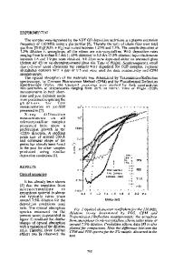
ABSTRACT We report on a study of ESR and conductivity on a series of hot-wire CVD microcrystalline silicon samples prepared with different hydrogen dilution of silane. We observe two different types of dangling bond defects in ESR in different microscopic environments. One type of defect is located at outer surfaces accessible to oxygen and/or chemicals, the other is located at inner boundaries presumably at columnar structures. We correlate changes of the defect density induced by either annealing, exposure to air or wet-chemical treatment with the morphology and electronic properties of the films. We find that annealing at 200 'C induces irreversible changes in donor concentration as monitored by an ESR signal at g = 1.9981±3. INTRODUCTION Microcrystalline silicon deposited by hot-wire CVD (HW pc-Si) is a promising material for thin film solar cells due to the high deposition rates obtained. To optimize HW pc-Si it is essential to understand the microscopic nature of defects and their influence on the electronic properties. Since the film quality is, among others, checked by conductivity measurements it is essential to have long-time stability of the film parameters. However, as was shown by Veprek and coworkers [1], the lateral conductivity of pc-Si films can be strongly affected by the interaction of the material with oxygen. The underlying microscopic nature of this effect, however, is still not completely understood. More recently it was argued by the Neuchatel group that also the incorporation of oxygen during film growth dramatically increases the dark conductivity of nominally undoped films [2]. In this report we investigate the behavior of pc-Si films on long-time exposure to air, annealing and wet-chemical treatment. We monitor the changes induced by the various treatments through ESR and conductivity measurements. The results will be discussed in a structural model of pc-Si consisting of inner and outer surfaces. SAMPLES AND EXPERIMENTAL DETAILS The pc-Si samples were deposited on Coming 7059 glass at a deposition temperature of 200 'C in an ultra-high vacuum hot-wire deposition system. Details are reported elsewhere [3]. The hydrogen dilution defined by the ratio of the hydrogen and silane gasflow rates, r = [H2 ]/[SiH4], amounted to 10, 15, and 30, respectively. In the following, we will refer to these three samples as low (L), medium (M) and high (H) dilution. The growth rate ranged from 5 to 7 A / s. The film thickness as measured by SEM is 4.9 pm (L), 3.9 prm (M), and 3.4 pm (H), and the crystalline volume fraction, X,, determined by Raman backscattering amounts to 53% (L), 64% (M), and 73% (H). As shown in Figure 1, the films clearly reveal columnar growth with 793
Mat. Res. Soc. Symp. Proc. Vol. 507 ©1998 Materials Research Society
Figure 1: SEM micrographs of sample L (left), M, and H (right) col
Data Loading...