Persistent Photocurrent in InP Nanowires Heteroepitaxially Bridged Between Single Crystal Si Surfaces
- PDF / 817,840 Bytes
- 7 Pages / 612 x 792 pts (letter) Page_size
- 90 Downloads / 285 Views
1080-O07-08
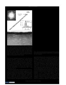
Persistent Photocurrent in InP Nanowires Heteroepitaxially Bridged Between Single Crystal Si Surfaces Ataur Sarkar1, M. Saif Islam1, Sungsoo Yi2, and A. Alec Talin3 1 Electrical and Computer Engineering, University of California, One Shields Avenue, Davis, CA, 95616 2 Molecular Technology Laboratory, Agilent Technologies, Currently at Advanced Laboratories, Philips Lumileds Lighting Company, San Jose, CA, 95131 3 Sandia National Laboratories, P.O. Box 969, Livermore, CA, 94551 ABSTRACT Room temperature photoelectrical characterization with 325-nm ultraviolet and 633-nm visible laser excitations is performed on lateral p-type InP nanowires bridged between vertically oriented heavily p-doped single crystal silicon electrodes. Experimental results under 5 V bias demonstrate persistent photoconductivity through a slow decay of excess photocurrent with relaxation times ~110 s and ~50 s for the UV and visible laser illuminations, respectively. Persistent photocurrent originates from the long recombination time due to carrier trapping in vacancies, defect centers, and surface states in the InP nanowires. The study opens a new understanding of trap physics of nanowire heterostructures, a critical investigation for applications of these materials in photonic devices. INTRODUCTION III-V semiconductor nanowires are highly promising for photonic applications because of their high carrier mobility and large optical absorption. High surface-to-volume ratio and, in some cases, ballistic transport properties of nanowires can dramatically enhance the performance of high-speed data communication systems through the use of nanowire-based photonic devices. Suitability of a photonic device for such high-speed data communication systems can be verified through photoelectrical characterization of the device. Nanowire-based devices must be well studied before selecting them for any photonic applications [1]. In applications, such as photodetectors, laser diode and modulators for high-speed optical data communication, the device must be highly responsive to photoexcitation and quickly relax to the dark state immediately after the light source is shut off. We investigated indium phosphide (InP) nanowires bridged between single crystal silicon electrodes and found that photogenerated excess carriers do not recombine immediately after the light source is turned off, rather the excess photocurrent decays slowly and it takes tens of seconds to reach the dark current level. The effect, called persistent photoconductivity (PPC), is observed when the charge carriers in a material are photoexcited above a ground energy state and they maintain the excited nonequilibrium state for a long time due to their delayed relaxation to the ground state [2-6]. PPC originates from the long recombination time due to carrier trapping. Surface states, vacancies, defect centers, dopants etc all can collectively contribute to the long trapping of photogenerated excess carriers and manifest as a temporary boost in dark conductivity, which may exist for da
Data Loading...