Properties of Zn Implanted GaN
- PDF / 1,163,812 Bytes
- 6 Pages / 414.72 x 648 pts Page_size
- 26 Downloads / 352 Views
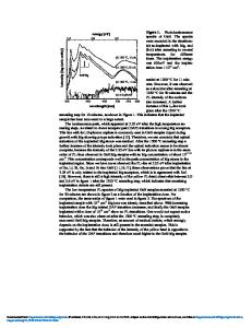
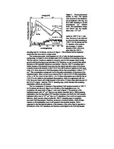
ABSTRACT We report the optical and structural properties of ion implanted GaN:Zn. Post-implant annealing up to 1100 'C was performed under flowing N2 in both a tube furnace and a rapid thermal annealing (RTA) system, with and without SiNx encapsulation layers. The implantation damage is quantified by transmission electron microscopy (TEM). Secondary ion mass spectroscopy (SIMS) detects significant rearrangement of implanted Zn only at the highest temperatures and doses investigated. Strain reduction, observed in GaN:Zn annealed at or above 975 'C by high-resolution x-ray diffractometry (HRXRD), indicates successful damage removal. The optical activation of annealed GaN:Zn is measured by photoluminescence (PL). The room temperature (RT) Zn acceptor transition at -430 nm is consistently observed in annealed GaN:Zn, but at low efficiency. We conclude that residual implantation damage and/or N loss during annealing limits the optical quality of implanted GaN:Zn. INTRODUCTION Ion implantation is widely used in semiconductor device technology to locally alter the electrical properties of materials, e.g. for doping or isolation. Less attention has been paid to ion implantation as a method for introducing optically active impurities. GaN LEDs can luminesce in any of the visible colors dependent on the dopant introduced [1]. If it is possible to realize good optical quality implanted GaN, LEDs would benefit from dopants incompatible with epitaxial growth processes. It would also be possible to fabricate monolithic multicolor LED arrays [2]. Two groups in the 1970's reported PL in ion implanted GaN. Pankove and Hutchby [3] implanted 35 different elements into GaN, reporting on GaN:Zn in detail [4]. Metcalfe et al. [5] investigated As and P doping. Each find that post-implantation annealing activates the dopants, but no estimates of the absolute PL efficiency are given. Our work evaluates ion implanted, annealed GaN:Zn for optical device applications. EXPERIMENT Our starting material was 1.5 pm GaN/sapphire MOVPE grown epilayers [6] having a background electron concentration of -1016 cm-3 which exhibit strong bandedge and negligible midgap PL. Zn+ ions were implanted up to 200 keV and Zn++ ions for 400 keV. Implanted samples were annealed (800 - 1100 0C) under flowing N 2 in a tube furnace (sample pairs face to face) or RTA, some with chemical vapor deposited SiN. encapsulation layers deposited after 795 Mat. Res. Soc. Symp. Proc. Vol. 395 01996 Materials Research Society
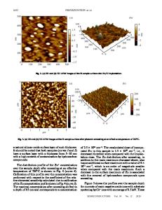
implantation, to inhibit N loss. GaN:Zn maintains its specular surface after 1 hr furnace anneals up to 1025 °C. At higher temperatures, unencapsulated samples decomposed leaving a liquid Ga surface. SiNx (10 - 50 nm) encapsulation permits annealing up to our experimental limit (1100 'C) without Ga droplet formation. However, above 900 'C, the SiNX encapsulation blisters badly, suggesting that significant N loss is occurring. A Cameca IMS 5f SIMS instrument rastered 8 keV 02+ or 17 keV Cs+ primary ions over (250 pm)2 to sputter flat bottomed craters. GaN:Z
Data Loading...