Photosensitive Amorphous Si Thin Films Prepared by Magnetron Technology.
- PDF / 36,323 Bytes
- 5 Pages / 595 x 842 pts (A4) Page_size
- 11 Downloads / 348 Views
M5.20.1
Photosensitive Amorphous Si Thin Films Prepared by Magnetron Technology. Galina Khlyap, Victor Brytan State Pedagogical University, 24 Franko str. Drogobych, 82100, Ukraine Larisa Bochkariova Jaroslavl State University, 4 Soviet str., Jaroslavl, 150014, Russia ABSTRACT Electric field – induced effects are studied in thin films of amorphous Si grown by magnetron sputtering performed in continuous and pulse modes. Current-voltage characteristics are measured under the room temperature in different spectral ranges. It is shown that the investigated dependencies are of exponential character in all range of applied bias. Good photosensitivity was revealed by the samples prepared in continuous mode in the near-IR and visible interval. The samples grown by the pulse magnetron technology were shown roomtemperature photosensitivity in near-IR range after 2000C hydrogenation. INTRODUCTION Amorphous silicon is an interesting material for new photonics and microelectronics. Thin film-based structures are seemed to be prospective objects for investigation and modeling operation of the active elements under various environmental conditions. The processes of charge carrier transfer in α-Si films and Me/α-Si structures are not studied well enough. This article presents results of measurements and analysis of the current-voltage characteristics (IVC) of the structures Al/α-Si obtained by magnetron sputtering in the range of current density from 10-9 up to 10-7 A/cm2 at room temperature. The main goal of the studies was to clarify the electron transport mechanisms in the film-based structures Al/α-Si under normal atmospheric conditions before and after hydrogenation performed during 24 h of annealing at 4000C under PH = 2500 Pa. EXPERIMENTAL DETAILS The investigated structures are plotted in the Fig.1.
(+) Al
(-)Al α-Si
glass
Figure 1. Schematic plot of the investigated samples.
M5.20.2
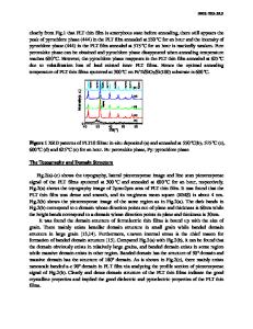
α-Si layers of 1 µm thickness were deposited on glass substrates by the magnetron sputtering method activated by plasma chemical decomposition of silane. Pulse alternating voltage of 55 Hz frequency was applied to two vertical plates. The layers were grown under pressure P = 70 Pa and temperature 2250C. Aluminum contacts with 1% Si impurity were deposited using mask of 1 mm diameter. Different room temperature IVC’s were measured under direct current. The similar studies were performed under UV-, near-IR and 100 Wt source illumination of the layers. The current-voltage dependencies shown below are obtained by measurements of the stationary current values under set values of the applied voltage. DISCUSSION Fig.2 plots experimental current-voltage dependencies of the investigated structures obtained under different light sources illumination.
1E-8
Current I, A
1 2 4 1E-9
1 - daylight 2 - 100 W light 3 - 760 nm light source 4 - 400 nm light source
3
1E-10 0
20
40
60
80
100
Applied voltage Va, V Figure 2. Room-temperature current-voltage characteristics of the examined samples. Experimental curves obtained under daylight (curve
Data Loading...