Plasma Enhanced Chemical Vapour Deposited Carbon Nanotubes for Field Emission Applications
- PDF / 1,737,919 Bytes
- 6 Pages / 612 x 792 pts (letter) Page_size
- 39 Downloads / 301 Views
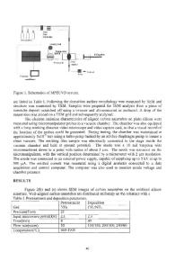
Plasma Enhanced Chemical Vapour Deposited Carbon Nanotubes for Field Emission Applications K. B. K. Teo, G. Pirio1, S.B. Lee2, M. Chhowalla, P. Legagneux1, Y. Nedellec1, D.G. Hasko2, H. Ahmed2, D. Pribat1, G.A.J. Amaratunga, and W.I. Milne. Engineering Department, Cambridge University, Trumpington St, Cambridge CB2 1PZ, UK 1 Thales Research and Technology, Domaine de Corbeville, 91404 Orsay Cedex, France 2 Microelectronics Research Centre, Cavendish Laboratory, Cambridge University, Madingley Road, Cambridge CB3 0HE, UK ABSTRACT Plasma Enhanced Chemical Vapour Deposition is an extremely versatile technique for directly growing multiwalled carbon nanotubes onto various substrates. We will demonstrate the deposition of vertically aligned nanotube arrays, sparsely or densely populated nanotube forests, and precisely patterned arrays of nanotubes. The high-aspect ratio nanotubes (~50 nm in diameter and 5 microns long) produced are metallic in nature and direct contact electrical measurements reveal that each nanotube has a current carrying capacity of 107-108 A/cm2, making them excellent candidates as field emission sources. We examined the field emission characteristics of dense nanotube forests as well as sparse nanotube forests and found that the sparse forests had significantly lower turn-on fields and higher emission currents. This is due to a reduction in the field enhancement of the nanotubes due to electric field shielding from adjacent nanotubes in the dense nanotube arrays. We thus fabricated a uniform array of single nanotubes to attempt to overcome these issues and will present the field emission characteristics of this. INTRODUCTION There is considerable interest in the application of carbon nanotubes for vacuum electron devices [1,2,3,4,5]. Carbon nanotubes have small diameters (few nanometers) and relatively long lengths (few microns), giving them a high aspect ratio and which can be usefully employed to generate a large electric field enhancement at their tips. Today, the common techniques for the preparation of nanotubes include high pressure arcs [6], laser ablation [7] and chemical vapour deposition (CVD) [8]. CVD growth is perhaps the most promising technique for the fabrication of electronic devices because carbon nanotubes can be deposited directly onto a substrate with high yield and uniformity. By simply patterning the catalyst using lithographic methods, it is possible to define exactly the position of nanotubes using CVD growth [9]. It was shown recently that aligned nanotubes have more desirable field emission characteristics [10] than nonaligned nanotubes. Plasma enhanced CVD (PECVD) is a feasible solution for the production of vertically aligned carbon nanotubes [11,12,13,14]. Hence, the aim of this paper is to provide an overview of the growth, electrical and field emission characteristics of PECVD grown vertically aligned carbon nanotubes. EXPERIMENTAL DETAILS The carbon nanotubes were produced using a dc-PECVD system which is described in detail elsewhere [14]. Briefly, the substrates are
Data Loading...


