Properties of InN grown by High-Pressure CVD
- PDF / 627,089 Bytes
- 6 Pages / 612 x 792 pts (letter) Page_size
- 81 Downloads / 460 Views
0892-FF06-02.1
Properties of InN grown by High-Pressure CVD Mustafa Alevli1, Goksel Durkaya1, Vincent Woods1, Ute Haboeck3, Hun Kang2, Jayantha Senawiratne1, Martin Strassburg1,2, Ian T. Ferguson2, Axel Hoffmann3, Nikolaus Dietz1,* 1 Georgia State University, Department of Physics and Astronomy, Atlanta, GA 30303, U.S.A. 2 Georgia Institute of Technology, School of ECE, Atlanta, GA 30332, U.S.A. 3 Technische Universität Berlin, Institut für Festkörperphysik, D - 10623 Berlin, Germany
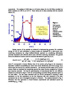
ABSTRACT Group III-nitride compound semiconductors (e.g. AlN-GaN-InN) have generated considerable interest for use in advanced optoelectronic device structures. The fabrication of multi-tandem solar cells, high-speed optoelectronics and solid state lasers operating at higher energy wavelengths will be made possible using (Ga1-y-xAlyInx)N heterostructures due to their robustness against radiation and the wide spectral application range. To date, the growth of indium rich (In1xGax)N films and heterostructures remains a challenge, primarily due to the large thermal decomposition pressures in indium rich group III-nitride alloys at the optimum growth temperatures. In order to control the partial pressures during the growth process of InN and related alloys, a unique high-pressure chemical vapor deposition (HPCVD) system with integrated real-time optical monitoring capabilities has been developed. We report initial results on InN layers grown at temperatures as high as ~850°C with reactor pressures around 15 bar. Such process conditions are a major step towards the fabrication of indium rich group III-nitride heterostructures that are embedded in wide band gap group III-nitrides. Real-time optical characterization techniques are applied in order to study the gas phase kinetics and surface chemistry processes during the growth process. For an ammonia to TMI precursor flow ratio below 500, multiple phases with sharp XRD features are observed. Structural analysis perform by Raman scattering techniques indicates that the E2 high mode improves as NH3:TMI ratio is decreased to below 500. Optical characterization of these InN layers indicates that the absorption edge shifts from down from 1.85 eV to 0.7 eV. This shift seems to be caused by a series of localized absorption centers that appear as the indium to nitrogen stoichiometry varies. This contribution will correlate the process parameters to results obtained by XRD, Raman spectroscopy and optical spectroscopy, in order to assess the InN film properties. INTRODUCTION Indium rich group III-nitride compound semiconductor heterostructures in conjunction with wide bandgap GaxAl1-xN layers have many potential applications for novel devices that are of significant importance due to their large spectral tunability. Device structures based on (Ga1-yxAlyInx)N heterostructures and related alloys will enable the fabrication of high efficiency, monolithic integrated energy conversion systems and high speed optoelectronic devices for optical communications. Presently, the growth of group III nitrides is d
Data Loading...