Properties of SiC-Based Luminescent Composite Thin Film As Light-Harvesting Material
- PDF / 970,044 Bytes
- 9 Pages / 612 x 792 pts (letter) Page_size
- 29 Downloads / 318 Views
HOTOCHEMISTRY AND MAGNETOCHEMISTRY
Properties of SiC-Based Luminescent Composite Thin Film As Light-Harvesting Material K. Benfadela, S. Kacia,*, L. Talbia, A. Keffousa, A. Benmounahb, I. Bozetinea, A. Boukezzataa, R. Rahmounea, Y. Ouadaha, L. Guerbousc, A. Kermada, S. Achachaa, B. Mahmoudia, and H. Cheragaa a
Research Center on Semiconductor Technology for Energetic, CMSI Division, CRTSE, 2 Bd Frantz Fanon, PB 140, 7M, Algiers, Algeria b Unité de Recherche (UR-MPE), Faculté des Sciences de l’Ingénieur, Cité Frantz Fanon, Université M’hamed Bougara de Boumerdès, Boumerdès, Algiers c Algiers Nuclear Research Center (CRNA), 2 Bd Frantz Fanon, BP 399, Algiers, Algeria *e-mail: [email protected] Received February 23, 2020; revised April 15, 2020; accepted April 15, 2020
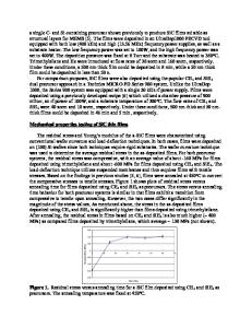
Abstract—In this study, we present the use of SiC/PVA composite thin films as downshifting layers (LDS) in order to improve the photoelectrical parameters of a Si-based solar cell. We showed that the adding of these layers increases the short circuit current density. This increase could surely lead to the improvement of the power conversion efficiency since the two parameters are relied. The J–V characterizations of the as made cSi solar cell measured under white light showed an enhancement of the photocurrent after coating the c-Si solar cell with SiC-based LDSs. The same behavior was noticed upon exposure to UV light illumination which depended strongly on the elaboration conditions of the luminescent porous SiC particles. A decrease in total reflectance of the c-Si solar cell coated with SiC based LDS was also observed. Spectral Response measurements have shown significant enhancement where the solar cells have poor optical response. Keywords: optical losses, c-Si, silicon carbide (SiC) particles, PVA, luminescent materials, luminescent down-shifting layers DOI: 10.1134/S0036024420130063
INTRODUCTION Crystalline silicon is the mainstream technology for photovoltaic energy conversion so far since 90% of the market use single crystal and multicrystalline silicon solar cells and will lead technology until the development of more cost effective PV technologies. Crystalline silicon is highly attractive as absorbers in mass produced, low cost and efficient solar cells. Two of the key attributes for efficient terrestrial solar cell operation are: (1) efficiently harvesting solar radiation across the entire solar spectrum and (2) minimization of parasitic charge carrier recombination. The 46.7% ultimate solar cell limit for direct solar irradiation can only be approached, once the cell is capable to focus all emitted photoluminescence back to the sun [1]. Recent studies showed that nanophotonic engineering could provide a pathway to approach the ultimate limit [1, 2]. Funnel-shaped silicon nanowire (SiNW) solar cells were introduced by and numerically analyzed. The funnel-shaped NW consisted of a cylinder over a conical unit. Its aim is to maximize the optical absorption over a large wavelength range and hence the elec-
trical efficiency by increasing t
Data Loading...