Pulsed Laser Annealing Effects in High Dose Rate Silicon Implants
- PDF / 1,101,079 Bytes
- 7 Pages / 415.8 x 637.2 pts Page_size
- 38 Downloads / 501 Views
1981 by Elsevier North Holland,
Inc.
Gibbons, Hess, and Sigron, eds. Laser and Electron-Beam Solid Interactions and M:aterials Processing
169
PULSED LASER ANNEALING EFFECTS IN HIGH DOSE RATE SILICON IMPLANTS
J.S. WILLIAMS, A. P. POGANY, D. G. BEANLAND R.M.I.T. Melbourne, 3000, Australia. D. J. CHIVERS, Harwell Research Laboratories, Didcot, England. M. J. KENNY, A. ROSE and M. D. SCOTT, AAEC Research Establishment, Lucas Heights, Australia.
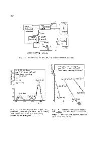
ABSTRACT High resolution Rutherford backscattering and channelling TEM and electrical measurements have been employed to investigate pulsed-ruby laser annealing effects in high dose rate ion implanted silicon wafers. The laterally non-uniform, part amorphous, part crystalline disordered structure which can result from high dose rate implants has been utilized to investigate the selective removal of amorphous or crystalline damage at near-threshold laser powers. Evidence is found for preferrential recrystallisation of amorphous damage regions over a broad laser power window which is below the threshold power required to melt adjacent crystalline silicon. At laser power levels above the crystalline-tomelt threshold, excellent uniformity in damage removal and electrical properties were obtained over the entire wafer.
INTRODUCTION High dose, high-dose-rate implantation into silicon can result in interesting damage non-uniformities across the target surface which arise from local heating effects during implantation. These damage variations are manifested as well defined colour bands observable across the wafer surface [1]. In some cases, the remnant damage can consist of part amorphous and part crystalline disorder, which 0 is difficult to remove at furnace anneal temperatures below 1100 C. In the pr sent paper, a pulsed ruby laser has been employed to anneal high dose rate As and P implanted silicon at various positions across the colourbanded surface. Of particular interest were the laser annealing conditions necessary to completely remove both amorphous and crystalline damage from the entire wafer, to provide uniform dopant profiles. Results demonstrated that excellent uniformity could be achieved across the wafer surface if the laserinduced melt depth extended beyond about three times the projected range of the implanted ions. At lower laser powers, close to the melt threshold, interesting preferrential damage-removal effects were observed, which provide evidence for a lower melting point of amorphous silicon in comparison with the crystalline phase [2]. EXPERIMENTAL A series of p-type 10-20 Qcm wafers were implanted with 40 keV As+ or P+ ions on the Lintott-Harwell ion implanter which utilizes mechanical scanning of targets. A 500 LA cm-2 dose rate was employed and implant doses were in the range 5 x 10¹⁵ to 5 x 10¹⁶ ions cm-. Clearly observable colour bands were produced across the wafer as a result of local heating effects occuring during high dose rate implants.
170 Following ion implantation, the targets were annealed at various positions across the wafers with resp
Data Loading...