Silicide Formation by Pulsed Excimer Laser Annealing
- PDF / 153,867 Bytes
- 6 Pages / 612 x 792 pts (letter) Page_size
- 33 Downloads / 420 Views
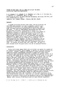
Silicide Formation by Pulsed Excimer Laser Annealing Connie Lew and Michael O. Thompson Department of Materials Science and Engineering, Cornell University, Ithaca, NY 14853 ABSTRACT Silicide formation may occur at the interface of metal and a-Si films upon annealing with a pulsed excimer laser (XeCl 308 nm; 30 ns). During laser-induced melting, the melt front reaches the Si/metal interface, where liquid phase kinetics allow reaction to occur to form a silicide, despite the > TM, a-Si, we are able to crystallize a-Si to poly-Si, but because the melt front cannot extend into the metal layer, no reaction takes place between the Si and metal. Therefore, the possible metal films that may be used are limited. Past studies of silicide formation of metal on Si were performed by both furnace anneal and pulse-laser anneal [4, 7-9]. Unlike furnace annealing, where silicide formation occurs by solidstate reaction and mass diffusion at temperatures of 200-900ºC to form uniform silicide compositions [7], silicides produced by pulsed-laser annealing occur by a non-equilibrium process of melt and rapid solidification. Formation times are on the order of the laser pulse duration (330 mJ/cm2, optical inspection shows Si film surface is damaged and roughened. The Si/W samples were able to sustain higher fluences before surface roughening. However, as observed in the RBS data in figure 2b, we again see no reaction take place at the Si/W interface when comparing the as-deposited sample to the samples laser annealed at varying Energy (MeV) 35
100
Ablation
Yield (#/uC/keV/msr)
Melt
Melt Duration (ns)
Crystallization
1/2
30
60
40
20
0
0.6
0.7
+
a-Si/W 80
0.5
0.92 MeV He 10 µC; 50° tilt
0.8
W
As-deposited 2 130 mJ/cm 2 263 mJ/cm 2 316 mJ/cm 2 334 mJ/cm
25 20 15 10
Si
5
0
100
200
300
400
500
2
0 200
250
300
350
400
Channel
Energy Density (mJ/cm )
Figure 2a. Melt duration as a function of laser fluence for a-Si/W on oxidized Si.
Figure 2b. RBS data of as-deposited and laser-annealed a-Si/W on oxidized Si. D5.22.3
fluences. We only see variation of the Si and W film thickness among the different samples. The roughening of the 334 mJ/cm2 Si/W sample is evident in the decrease in yield count of the Si peak and the broadening of the W peak towards the sample surface, as previously observed in the ablated Si/Al/Cr sample. We conclude that film damage occurs before the onset of W melt. a-Si/Ti For e-beam evaporated a-Si (120 nm)/Ti (140 nm) on oxidized (700 nm) Si wafer, melt initiates at ~120 mJ/cm2 (figure 3a). The melt duration increases from 35 to 80 ns as laser fluence increases from 120 to 280 mJ/cm2. From 290 to 310 mJ/cm2, the Si surface ablates, as observed by optical inspection and by dramatic decrease in surface reflectance signal. However, melt may continue beyond this point at energy densities >320 mJ/cm2, until at fluences of >390 mJ/cm2, film ablation occurs again. This suggests that at the intermediate energy density of ~300 mJ/cm2, the melt front has reached the Si/Ti interface, but T
Data Loading...