A nonparabolic conduction band study of circular quantum dot optical properties: modeling of surface roughness by using
- PDF / 3,807,425 Bytes
- 10 Pages / 547.087 x 737.008 pts Page_size
- 2 Downloads / 216 Views
RESEARCH PAPER
A nonparabolic conduction band study of circular quantum dot optical properties: modeling of surface roughness by using Koch snowflakes M. Solaimani
&
Abdolreza Rasouli Kenari
Received: 28 March 2020 / Accepted: 3 August 2020 # Springer Nature B.V. 2020
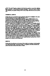
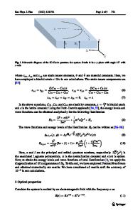
Abstract In this work, we investigate the optical properties of single and multiple quantum dots (QDs) based on AlxGa1-xAs/GaAs with two Koch snowflake-shaped and circular geometries. The idea is to determine the impact of the surface roughness of the circular QDs on the mentioned optical properties. This is an important issue in designing optoelectronic devices (e.g., photodetectors or light-emitting systems) because the position and magnitude of the absorption coefficient play important roles in devising them. We have also studied the effects of the conduction band nonparabolicity, QD size, number of QDs, and composition parameter x on the absorption coefficient. For this purpose, we have used an efficient finite difference method to solve the twodimensional Schrodinger equation. The computational algorithm of the Koch snowflake-shaped QD production is also described.
M. Solaimani (*) Department of Physics, Faculty of Science, Qom University of Technology, Qom, Iran e-mail: [email protected] A. R. Kenari Faculty of Electrical and Computer Engineering, Qom University of Technology, Qom, Iran
Present Address: M. Solaimani Department of Physics, Faculty of Mechanical Engineering, Qom University of Technology, Qom, Iran
Keywords AlxGa1-xAs/GaAs Koch snowflake-shaped and circular single and multiple quantum dots (QDs) . Efficient finite difference method . Conduction band nonparabolicity . Nanostructures
Introduction Bulk semiconductor materials are potentially sensitive to absorb or emit a large portion of the electromagnetic spectrum. By reducing the carrier’s confinement to three dimensions, the QDs generate and intersubband transitions are allowed. During the last few years, there has been a growing interest in the study of QDs. These structures behave like artificial atoms with outstanding optoelectronic properties. Nowadays, QDs have found vast applications in modern technologies such as amplifiers (Borri et al. 2000), photodetectors (Hellström et al. 2010), photodiode (Ji et al. 2008), memories (Nilsson et al. 2006), nanolasers (Gonzalez et al. 1999a), charge qubits (Hentschel et al. 2007), solar cells (Linares et al. 2011), transistors (Cervenka et al. 2011), and waveguides (Ma and John 2011). To make a better comparison between modern technologies with and without QDs especially in plasmonic devices, one can see Refs. (Gerislioglu et al. 2020a, b; Gerislioglu and Ahmadivand 2020). The effect of conduction band nonparabolicity on the optical properties of semiconducting heterostructures has less been investigated. However, there are illustrative papers that investigate this issue (Riffe 2002) or reveal the effect of this parameter on the physical
242
Page 2 of 10
properties of a quantum system. Influence of the nonparabolicity on t
Data Loading...