A Novel Direct Pulse Laser Deposited Nickel Silicide Ohmic Contact to n -SiC
- PDF / 1,774,089 Bytes
- 6 Pages / 612 x 792 pts (letter) Page_size
- 79 Downloads / 282 Views
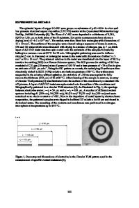
A Novel Direct Pulse Laser Deposited Nickel Silicide Ohmic Contact to n-SiC M.W. Cole, P.C. Joshi, C. W. Hubbard, E. Ngo, J.D. Demaree, J.K. Hirvonen, M. C. Wood and M.H. Ervin US Army Research Laboratory, Weapons and Materials Research Directorate Aberdeen Proving Ground, MD 21005, U.S.A. ABSTRACT Pulsed laser direct deposit Ni 2Si Ohmic contacts were successfully fabricated on n-SiC. The electrical, structural, compositional, and surface morphological properties were investigated as a function of heat treatments ranging from 700 ˚C to 950 ˚C. The as-deposited and 700 ˚C annealed samples were non-Ohmic. Annealing at 950 Co yielded excellent Ohmic behavior, an abrupt void free interface, and a smooth surface morphology. No residual carbon was present within the contact film or at the film-SiC interface and the contact showed no appreciable contact expansion as a result of the 950 ˚C annealing process. Results of this investigation demonstrate that 950 ˚C annealed pulse laser deposited Ni2Si-SiC contacts possess excellent electrical, interfacial, microstructural, and surface properties, which are required for reliable device operation. INTRODUCTION SiC is an important material for high temperature, high power and high frequency semiconductor device applications due to its exceptional properties, such as, wide energy bandgap, high electric breakdown field, high thermal conductivity, large saturated electron drift velocity [1-5]. In order to realize these superior properties for the next generation of devices low resistance, thermally stable, reliable metallizations for Ohmic contacts must be developed. Recently, there have been a considerable number of research efforts focused on the development of Ohmic contacts to n-SiC. As a result of these studies Ni-based Ohmic contacts have been suggested as -6superior2 candidates due to their reproducible low specific contact resistance, less than 5.0 x 10 Ω-cm , and good physical thermal stability at temperatures up to 500˚C [6-9]. It has been demonstrated that the excellent Ohmic behavior is due to the formation of Ni-silicide after high temperature annealing at 950-1000 ˚C [4, 10-13]. Unfortunately, the formation of the Ni-silicide, with its desirable low specific resistance, is paralleled by several undesirable features. These features include broadening of the metal-SiC interface, a rough interface morphology heavily laden with Kirkendall voids, carbon segregation at the metal-SiC interface and/or throughout the metal layer, and substantial roughening of the contact surface [4, 11, 12, 14]. Thus, even though Ni contacts possess excellent electrical properties, the above mentioned features will lead to device reliability problems and ultimately cause device failure via contact degradation and/or wire bond failure after exposure to long term high power and high temperature device operational stresses. Improved material properties, with respect to pure Ni contacts, has been demonstrated utilizing high temperature (950 ˚C) annealed Ni/Si multi-layers on SiC [12, 15]. The conce
Data Loading...