An investigation of a nonspiking Ohmic contact to n-GaAs using the Si/Pd system
- PDF / 6,260,525 Bytes
- 9 Pages / 593.28 x 841.68 pts Page_size
- 88 Downloads / 296 Views
. Sands Bell Communications Research Inc., Red Bank, New Jersey 07701
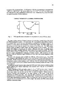
T.F. Kuech IBM, Thomas J. Watson Research Laboratory, Yorktown Heights, New York 10598 (Received 29 January 1988; accepted 9 June 1988) A low-resistance nonspiking Ohmic contact to «-GaAs is formed via solid-state reactions utilizing the Si/Pd/GaAs system. Samples with Si to Pd atomic ratios greater than 0.65 result in specific contact resistivity of the order of 10^ 6 O cm2, whereas samples with atomic ratios less than 0.65 yield higher specific contact resistivities or rectifying contacts. Rutherford backscattering spectrometry, cross-sectional transmission electron microscopy, and electron diffraction patterns show that a Pd2Si layer is in contact with GaAs with excess Si on the surface after the Ohmic formation annealing. This observation contrasts with that on a previously studied Ge/Pd/GaAs contact where Ohmic behavior is detected after transport of Ge through PdGe to the interface with GaAs. Comparing the Ge/Pd/GaAs system with the present Si/Pd/ GaAs system suggests that a low barrier heterojunction between Ge and GaAs is not the primary reason for Ohmic contact behavior. Low-temperature measurements suggest that Ohmic behavior results from tunneling current transport mechanisms. A regrowth mechanism involving the formation of an n * GaAs surface layer is proposed to explain the Ohmic contact formation.
I. INTRODUCTION The formation of a nonspiking Ohmic contact to nGaAs based on solid phase epitaxy has been investigated recently. It was found that specific contact resistivity, pc of the order of 1 to ~ 2 X l O ~ 6 O era2 on «-GaAs ( ~ 1 X 1018 cm" 3 ) can be achieved reproducibly using the Ge/PdGaAs system.' '2 The contact scheme involves the deposition of a metallic-transport medium Pd onto which a layer of amorphous Ge is then deposited without breaking vacuum. The thickness of the Pd is not critical and is usually in the range of 250-1500 A. The thickness of the Ge should be chosen such that, upon annealing, there is enough to react with the entire layer of Pd with ~ 500 A excess Ge remaining. The Ohmic contact formation was explained in terms of a replacement mechanism2 as follows. Initially, elemental Pd is in contact with the GaAs substrate and with amorphous Ge on top. Upon annealing, the Pd layer reacts with Ge to form Pd 2 Ge and then PdGe. A very limited reaction occurs in the initial stage of annealing at the Pd/GaAs interface, forming a ternary compound Pd x Ga J ,As z (x~4,.y~ l , z ~ 1), which is usually found tobeGa-rich (ykz) .3-4 After annealing at 325 °C for 30 min, the Pd has been completely consumed to form PdGe. The excess Ge is transported across the germanide to grow epitaxially on the GaAs substrate due to the lower free 922
J. Mater. Res. 3 (5), Sep/Oct 1988
http://journals.cambridge.org
energy of Ge in the crystalline state compared to that in its amorphous state. In the meantime, Ge may diffuse into the GaAs substrate at dopant levels to form an n + surface layer due to the existence of excess Ga vacancies i
Data Loading...