A Study on Hysteresis Effect of Barium Strontium Titanate Thin Films for Alternative Gate Dielectric Application
- PDF / 1,276,947 Bytes
- 6 Pages / 415.8 x 637.2 pts Page_size
- 105 Downloads / 376 Views
269
Mat. Res. Soc. Symp. Proc. Vol. 606 0 2000 Materials Research Society
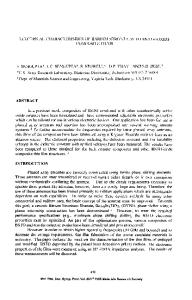
EXPERIMENTS P-Si (100) wafers with a resistivity of 5-25Q2.cm were used as the substrate. Field oxide of 3500-4000A was grown, patterned using photolithography, and etched in buffered HF solution to form the active area. Prior to BST deposition, the Si wafer was piranha cleaned and HF (1:40) dipped. BST film was then RF sputtered from a stoichiometric target with a composition of Ba 0.5Sr 0.5Ti0 3. The base pressure of the sputter chamber was about 5x10 7 Torr, and the deposition temperature was 460'C. The sputtering procedure consisted of two steps to improve the BST/Si interface: a low power sputter at 20W followed by a higher power sputter at 50W. In some structures, Ta2 0 5 (35A-75A) were DC reactive-magnetron sputtered in an Ar+0 2 ambient to serve as a barrier layer. Pt (1500A) was used as the top electrode. Pt was sputtered, patterned using photolithography, and etched using aqua regia solution (H2 0:HCI:HNO 3 = 5:7:1) at 80'C. The area of the capacitor is 5xIO-5 cm 2. Annealing in N 2 or 02 ambient was then performed in a conventional furnace. The Capacitance-Voltage (C-V) characteristics and hysteresis were measured using HP (Hewlett Packard) 4194, and the charge trapping property was measured using HP 4156. RESULTS AND DISCUSSIONS Fig. 1 demonstrates a typical C-V hysteresis loop of the Pt/BST/Si structure. A counterclockwise hysteresis loop can be seen. It is known that at room temperature the BST film is in a paraelectric phase [11] and indeed P-E (Polarization vs electric field) measurement of the Pt/BST/Ir (MIM) structure indicates no polarization hysteresis (not shown). To further understand the difference between Ir and Si substrate, the crystallinity of BST films on Ir and Si was examined. Glancing angle (50) X-ray diffraction results are shown in Fig. 2. It can be seen that BST films show the same polycrystalline structure. Fig. 1 shows that the C-V hysteresis can be significantly reduced by thermal annealing, although the capacitance also drops, indicating an increase of the equivalent oxide thickness. This increase has been reported to be due to the interfacial layer growth [12]. The "counterclockwise" behavior and thermal annealing effect observations rule out ferroelectricity as the cause of hysteresis for these films. They suggest an improvement of the BST/Si interface during the annealing. Also, note the C-V curves shift almost parallel to each other, which seems to indicate that the hysteresis is not due to the interface states. 6 10-11
....
..
5 10"
......
BST/Siz
2))
ac 310-1
0 5l 3--- 800 C. N6,
a2 2
0
*0-1 -700 C, N, 5'
0 ...600 C, N, 5' 5 o~c 0lo-ot ........
1101
-5
-4
-3
-2
..
.A
2'
-1
..
0
&.....
1
2
10
Gate Voltage (V )
20
30
40
50
60
20
Fig. 1. Typical hysteresis behavior of Pt/BST/Si, counterclockwise loop can be seen and thermal annealing reduces hysteresis.
270
Fig. 2. Glancing angle (50) XRD patterns show similar crystallinity for BST on Ir and Si.
The hysteresis
Data Loading...