Activation Enthalpy of Sb Diffusion in Biaxially Compressed SiGe Layers
- PDF / 397,489 Bytes
- 6 Pages / 420.48 x 639 pts Page_size
- 55 Downloads / 328 Views
ABSTRACT Enhanced Sb diffusion in biaxially compressed Si,.-Gex layers is observed. Assuming the prefactors to be stress independent the Sb diffusion coefficients in biaxially compressed Sio.9 Geo., and Sio and 0 gGeo. 2 were extracted as 0.4x 10² exp[- (3.98(eV) ± 0.12)/kT]
1.3x
102 exp[- (3.85(eV)
±0.12)/kT] cm 2 /s,
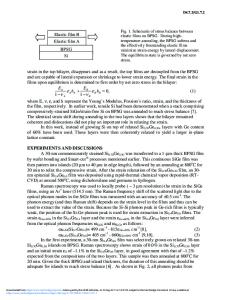
respectively. The activation volume of Sb diffusion in Sil,.Gex (x < 0.2) is estimated to be close to Q, where Q is the volume corresponding to a silicon lattice site. INTRODUCTION Along with the traditional application of the "external" pressure', the modern technology provides excess to strained semiconducting heterostructures where the pressure (stress) is generated "internally" due to the lattice mismatch at the heterointerface. Presently, this type of samples are used to extract the characteristic parameters of impurity- and self-diffusion in 2 semiconducting materials. The main target of the present contribution is to determine the activation enthalpies of Sb diffusion in strained Sil.,Ge. epilayers (AH) and to extract the activation volumes of the Sb diffusion (AV) in these layers. To reach this target Sb diffusivities were measured in strained SilxGe, epilayers and 3subsequently compared to that in unstrained layers with the same composition of Sil-,Ge,. EXPERIMENTAL Samples and anneals Heterostructures with strained epitaxial Si-.,Ge, (x 5 0.3) were grown by Molecular Beam Epitaxy (MBE) in a VG-80 system on Si, (100)-oriented n' substrates. First, a -100 nm thick undoped and, subsequently, a -300 nm Sb doped Si-buffer layer were deposited on the substrate. The Sb concentration was kept constant at - 1019 cm 3 throughout the doped layer. Further, undoped Si0.9Ge 0.1, Sio.8Ge 0 .2 or Si 0.7Ge0 .3 spacers, 40, 35, and 30 nm thick, were deposited to accommodate Sb out diffusion from the Si-buffer layer. The use of these diffusion structures (with relatively thin Sil,,Ge. spacers) made it possible to perform high temperature diffusion anneals without strain relaxation of Sil-,Ge, layers. 4 Furthermore, the wafers were capped with a -100 nm silicon layer to increase the thermal stability of the structures. 5 A fraction of each wafer was not subjected to any further annealing and was used to measure the initial dopant and Ge profiles. To study Sb diffusion, the samples were heat treated in a vacuum furnace (10-7 Torr range) in the temperature range from 740 to 925 °C with an accuracy of ± 2 °C for a given 213 Mat. Res. Soc. Symp. Proc. Vol. 532 01998 Materials Research Society
temperature. Long timeofanneals were used order totemperatures minimize thewere errordifferent related for to the heating/cooling stages < 5 minutes. The inannealing structures with different composition of the strained Sil.xGex layers. For the samples with higher Ge content the lower temperatures were used (in order to avoid stress relaxation and, in fact, because of rather fast Sb diffusion through the thin Si0.sGe0.2 and Si0.TGe0.3 spacers). Structural characterization Extensive structural characterization of both vir
Data Loading...


