Advanced microelectromechanical systems-based nanomechanical testing: Beyond stress and strain measurements
- PDF / 2,478,872 Bytes
- 7 Pages / 585 x 783 pts Page_size
- 25 Downloads / 264 Views
Introduction
In situ tensile tests
A growing number of in situ electron microscopy nanomechanics investigations now rely on microelectromechanical systems (MEMS), from instrumented, active MEMS devices, arrays of passive MEMS structures, or passive “push-to-pull” (PTP) MEMS combined with a nanoindentation transmission electron microscope (TEM) holder.1–9 These MEMS setups are ideal experimental platforms to simultaneously quantify mechanical properties and to characterize microstructure evolution at the nanometer scale. They can be supplemented and enriched with atomistic models to provide thorough understanding of defect mechanics.10–13 So far, most of these studies have focused on elastic and plastic deformation under simple monotonic loadings. This article provides an overview of current efforts to perform in situ advanced nanomechanical tests for fracture, fatigue, wear, and other properties using integrated micro-/ nanofabrication. With these setups, a thorough nanoscale understanding of defect mechanics under complex loading modes (e.g., cyclic, high strain rates, multiaxial), in highly localized regions (i.e., shear instabilities, crack tip, sample surface), and in various reactive environments is now within reach.
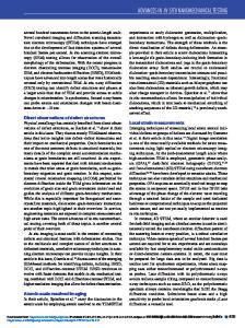
In situ electron microscopy mechanical and electromechanical testing of materials based on MEMS devices, such as the one shown in Figure 1a, has been a powerful approach to unambiguously establish structure–property relationships in low-dimensional metallic and semiconducting materials.2,7 By integrating microscale electronic actuation (with nanometer resolution) and load sensing (with nN resolution), simultaneous acquisition of high-resolution images of the atomic structure of tested specimens during the testing was achieved. This enabled direct imaging of deformation and failure processes with unprecedented resolution.14 For instance, the first direct correlation between failure stress and number of failed shells in multiwalled carbon nanotubes was obtained, which resolved literature discrepancies between theoretical quantum mechanical predictions and experimental measurements of Young’s modulus and strength.15 Intershell cross-linking effects, as a function of electron radiation dose, were also revealed in the multiwalled carbon nanotubes.14,15 By incorporating feedback control schemes in the MEMS devices, both load and displacement control experiments can be performed. The displacement control tensile testing capability
Sanjit Bhowmick, Bruker Nano Inc., USA; [email protected] Horacio Espinosa, McCormick School of Engineering and Applied Sciences, Northwestern University, USA; [email protected] Katherine Jungjohann, Center for Integrated Nanotechnologies, USA; [email protected] Thomas Pardoen, Institute of Mechanics, Materials and Civil Engineering, Universite Catholique de Louvain, Belgium; [email protected] Olivier Pierron, Woodruff School of Mechanical Engineering, Georgia Institute of Technology, USA; [email protected] doi:10.1557/mrs.2019.123
48
Data Loading...