Analytical and mechanical evaluation of diamond films on silicon
- PDF / 4,792,243 Bytes
- 10 Pages / 593.28 x 841.68 pts Page_size
- 27 Downloads / 426 Views
I. INTRODUCTION
Diamond is the hardest of all naturally occurring materials, is one of the most chemically inert materials, and has the highest room temperature thermal conductivity of any material.1'2 The hardness of diamond is also accompanied by a low wear rate, and diamond surfaces can have low friction coefficients.2"4 These properties make diamond films excellent candidates for tribological coatings in harsh environments. Tribological studies of diamond have shown correlations of friction and wear behavior with direction of sliding, ambient testing environment, and surface topography.3'4 However, there has been very little tribological characterization of diamond films, or even diamond-like films, in controlled studies where the effects of parameters such as contact coupling material, testing environment, or film treatment could be examined. We are in the process of beginning such tribological studies of diamond films. Prior to beginning these tribological studies, we have characterized a diamond film commercially deposited on silicon by a variety of analytical and mechanical procedures. These preliminary studies had two goals: (1) to identify the quality and characteristics of the commercially obtained diamond film; and (2) to establish methods of analyzing diamond films which
minimize surface damage and maximize chemical state information. This paper addresses the first goal. II. SAMPLE PREPARATION
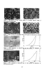
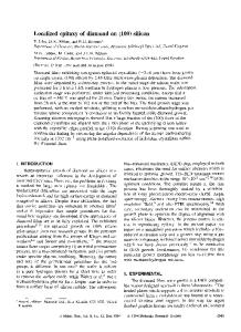
A diamond thin film was commercially deposited onto a polished 10 cm diameter silicon (100) wafer by a plasma enhanced chemical vapor deposition process, utilizing a thin diamond-like carbon film at the interface for improved adhesion.5 The film thickness was measured with a Sloan Dektak 3030 profilometer, using a vertical resolution of 0.1 nm and a 20 mg (0.2 mN) load with a standard 12.5 jtun radius diamond stylus. The film averaged roughly 2.3 nm. thickness near the center of the wafer, gradually increasing to about 2.7 nm thickness near the edge of the film. Measurements at the edge of the film were made where the film did not extend to the edge of the wafer; measurements at the center of the wafer were made from locations where the film spalled from the substrate during the process of sectioning the wafer (see below). To evaluate sample uniformity and to accommodate many different measurements, the silicon wafer was sectioned into 12 mm x 12 mm squares. Each square was numbered and assigned to a zone. Figure 1 shows the sample numbering and zonation. Those sam2589
J. Mater. Res., Vol. 5, No. 11, Nov 1990
http://journals.cambridge.org
Downloaded: 13 Mar 2015
IP address: 132.174.255.116
D. E. Peebles and L. E. Pope: Analytical and mechanical evaluation of diamond films on silicon
IV. ATOMIC FORCE MICROSCOPY
A
A
/
1
10
4
3
2
1
9
8
7
6
S 5
A"
- Outer
16 15 14 13 12 11
?2 21 20 19 18 17
\N
28 27 26 25 24 23
s
32 31 30 29
J
Edge
Intermediate j— Center
V/
FIG. 1. Schematic of the diamond-coated silicon (100) wafer, showing the numbering scheme of the 12 mm x 12 mm samples, and i
Data Loading...