ARC Discharge for the Synthesis of Monoclinic Ga 2 O 3 Nanowires
- PDF / 970,472 Bytes
- 5 Pages / 417.6 x 639 pts Page_size
- 43 Downloads / 243 Views
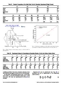
and Ni:Co:Y=4.5:4.5:I) was pressed into a small hole (diameter:4 mm, depth:25 mm) of the graphite anode (diameter:6 mm). DC current of 55-65 A with a voltage of 13-15 V was applied between two electrodes under a total pressure of 500 torr of argon and oxygen gases (pA:po2=400:100). Arching time was typically 5-6 sec. The chamber wall was kept cooled by circulated water. Scanning electron microscope (SEM) and high-resolution transmission electron microscope (HRTEM) were used to investigate the morphology and the microstructure of nanowires. X-ray diffraction (XRD) and Fourier transformed (FT) Raman spectroscopy were employed to confirm P-Ga 20 3 structure. UV adsorption measurement was done for determining optical band gap. RESULTS AND DISCUSSION Nanowires were deposited on the cathode, chamber wall, and in-between as a form of web-like network. Bluish grey powders were obtained from three regions, although original GaN powder was white in color. In addition, small amount of carbon nanotubes were detected sometimes as a black powder. Therefore, a careful control of arcing time was required to minimize the production of carbon nanotubes. The pressure is also a very important factor for forming nanowires. We could not obtain the nanowires at pressures under 450 torr. Bluish grey powders were extracted exclusively for characterizations.
(a))
o
-__• :"1
4
(A)
[0011 Fig. I.(a) SEM image of Il-Ga 2O3 nanowires, (b) HRTEM image of I3-Ga 2O3 nanowire, (c)Simulated image of 11Ga2O3 nanowires with 6×6× 12 supercell. Figure 1(a) shows a typical SEM image from web-like network. A large quantity of nanowires are formed with relatively uniform diameters. The nanowires are straight and long, resulting in large aspect ratio. We observed from cathode deposits that nanowires are as long as one hundred micrometer, in some cases [41. In this case, very pure nanowires were obtained, in contrast with carbon nanotubes generated by arc discharge where large amount of nanoparticles were produced in addition to carbon nanotubes [5]. We found that addition of small amount of yttrium was necessary for massive production of nanowires, suggesting that yttrium may play as an effective catalyst. Note that no nanowire was formed without transition metals. Figure 1(b) shows a HRTEM image of the nanowire. The image clearly illustrates crystalline structure of nanowire with twin defects (twin angle of about 1600) at the center of the nanowire. The nanowire reveals a smooth surface without step edges. The typical diameter of the nanowires is about 33 nm. Note that no amorphous layer was formed on the surface. The inset shows the Fourier diffractogram obtained from the HRTEM image, indicating a crystalline
240
nature and the direction of the nanowire axis to be [001]. In order to confirm these, we constructed a monoclinic Ga2 0 3 nanowire and obtained simulated pattern for the HRTEM image, as shown in Fig. 1(c), again clearly demonstrating the similar properties. The crystallographic directions in the simulated pattern agree with the observed H
Data Loading...


