Atomic Force Microscope Observation of Growth and Defects on As-Grown (111) 3C-SiC Mesa Surfaces
- PDF / 1,694,840 Bytes
- 6 Pages / 612 x 792 pts (letter) Page_size
- 42 Downloads / 352 Views
J5.32.1
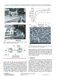
Atomic Force Microscope Observation of Growth and Defects on As-Grown (111) 3C-SiC Mesa Surfaces Philip G. Neudeck, Andrew J. Trunek1, and J. Anthony Powell2 NASA Glenn Research Center, 21000 Brookpark Road, M.S. 77-1, Cleveland, OH 44135, USA 1 OAI, NASA Glenn, 21000 Brookpark Road, M.S. 77-1, Cleveland, OH 44135, USA 2 Sest, Inc., NASA Glenn, 21000 Brookpark Road, M.S. 77-1, Cleveland, OH 44135 USA ABSTRACT This paper presents experimental atomic force microscope (AFM) observations of the surface morphology of as-grown (111) silicon-face 3C-SiC mesa heterofilms. Wide variations in 3C surface step structure are observed as a function of film growth conditions and film defect content. The vast majority of as-grown 3C-SiC surfaces consisted of trains of single bilayer height (0.25 nm) steps. Macrostep formation (i.e., step-bunching) was rarely observed, and then only on mesa heterofilms with extended crystal defects. As supersaturation is lowered by decreasing precursor concentration, terrace nucleation on the top (111) surface becomes suppressed, sometimes enabling the formation of thin 3C-SiC film surfaces completely free of steps. For thicker films, propagation of steps inward from mesa edges is sometimes observed, suggesting that enlarging 3C mesa sidewall facets begin to play an increasingly important role in film growth. The AFM observation of stacking faults (SF’s) and 0.25 nm Burgers vector screw component growth spirals on the as-grown surface of defective 3C films is reported. INTRODUCTION The growth of high-quality 3C-SiC heteroepitaxial films on top of arrays of mesas etched into commercial on-axis wafers has recently been reported [1-5]. In particular, growth by the “step-free surface heteroepitaxy” technique has achieved 3C-SiC mesa films entirely free of stacking fault (SF) and double-positioning boundary (DPB) defects on the majority of 4H/6HSiC mesas that are free of substrate screw dislocations (SD’s). However, only two initial AFM scans of as-grown 3C mesa film surfaces have been published to date [5]. This paper presents more extensive AFM observations of as-grown (111) 3C-SiC mesa heterofilm surfaces. EXPERIMENTAL The experimental processes for achieving and characterizing high-quality 3C-SiC heterofilm growth (including polytype confirmation by multiple independent techniques) on top of arrays of mesas patterned into commercial 4H/6H on-axis wafers have been detailed previously [1-5]. Table I describes specific growth process variations applied to the samples reported in this paper. The 4H-SiC substrates with patterned mesas were placed into a horizontal flow epitaxial reactor and subjected to a pre-growth high temperature etch in either HCl or H2. It should be noted that the uncoated graphite in the reactor supplies additional carbon to the growth environment, as we have observed SiC growth even when propane flow is reduced to zero. The top surfaces of mesas that were free of SD’s were then rendered completely free of atomic scale steps by carrying out
J5.32.2
homoepitaxial growth a
Data Loading...