Challenges in Interface Trap Characterization of Deep Sub-Micron Mos Devices using Charge Pumping Techniques
- PDF / 1,581,046 Bytes
- 14 Pages / 415.8 x 635.4 pts Page_size
- 55 Downloads / 410 Views
ABSTRACT This work surveys some of our recent experimental and theoretical advances in charge pumping for the electrical characterization of interface traps present in MOSFET architectures. The first part of this paper is devoted to an improved time-domain analysis of the charge pumping phenomenon. This approach presents the main advantage to use the same formalism to describe the charge pumping contribution of a single trap or a continuum of traps at the Si-Si0 2 interface. The implications for deepsubmicron MOSFET characterization are illustrated. Some experimental aspects are then presented, including the adaptation of the technique to ultra-thin oxides, non-planar oxides and DRAM memory cells. Finally, recent charge pumping characterization results are reported concerning the electrical behavior of the Si-Si0 2 interface submitted to particular technological treatments, electrical and radiation stresses, or post-degradation anneals.
INTRODUCTION With the ever shrinking of device dimensions, deep sub-micron MOS transistors enter now in a critical range where quantum-confinement effects, tunneling leakage mechanisms and single-trap activity make their characterization more and more difficult from the electrical point-of-view. This is particularly true for the characterization of the Si-Si0 2 interface in such ultra-thin MOS systems, which require the development of new experimental approaches to correctly probe interface and near-interface traps [I ]. The aim of this contribution is to review some of our recent experimental and theoretical developments concerning the charge pumping (CP) techniques, recognized from the two last decades as powerful tools for the characterization of dielectric-silicon interfaces in a wide variety of advanced devices [2]. This family of techniques is based on the exploitation of a repetitive process whereby majority carriers coming from the substrate recombine with minority carriers previously trapped in interface states, when the MOS transistor is submitted to well-chosen biasing cycles. By taking into account the emission processes, which control the exchange of charges at the interface, interface trap characteristics such as the density and the capture cross sections for electrons and holes can be obtained. This survey particularly focuses on the way to adapt CP techniques and extraction models in the case of ultra-thin oxides or non-planar interfaces. Results concerning the electrical activity of the Si-SiO2 interface, deduced from these techniques, are reported. We begin this review by presenting a comprehensive description of the CP phenomenon based on an improved time domain analysis considering the time- and energy-resolved evolutions of the trap filling probability in the semiconductor bandgap. Such a numerical approach is shown to be a powerful tool to extract parameters related to single or distributed interface traps.
THEORY The accurate modeling of CP techniques is a key-issue for the characterization of individual traps in MOSFETs. This aspect has been recently pointed
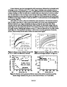
Data Loading...