Chemical Beam Epitaxy of GaP Using Triethylgallium and Tertiarybutylphosphine
- PDF / 1,250,591 Bytes
- 6 Pages / 420.48 x 639 pts Page_size
- 39 Downloads / 304 Views
CHEMICAL BEAM EPITAXY OF GaP USING TRIETHYLGALLIUM AND TERTIARYBUTYLPHOSPHINE
James T. Kelliher and Klaus J. Bachmann North Carolina State University, Department of Materials Science and Engineering, Box 7919, Raleigh, NC 27695-7919. ABSTRACT: In this paper we report the growth of GaP/Si heterostructures by metalorganic chemical beam epitaxy (MOCBE), including information on a MOCBE system custom built for this work. The gallium source was triethylgallium and the phosphorus source was tertiarybutylphosphine. The range for GaP epitaxy is 260 < T < 3750C.
Methods of characterization included scanning electron microscopy
(SEM), Auger electron (AES), X-ray photoelectron (XPS) and Rutherford backscattering (RBS) spectroscopies. INTRODUCTION:
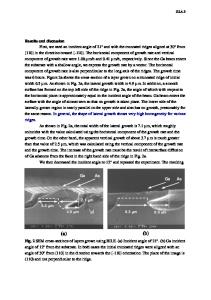
The motivation for this work is the possible utility of GaP for dielectric isolation of silicon, because its wide bandgap and electron affinity difference with regard to silicon provide for a sufficient barrier to majority carrier flow. Also, the lattice constants nearly match at room temperature and the tetrahedral coordination in both lattices should permit excellent interface properties to be maintained. Triethylgallium and tertiarybutylphosphine are used as source materials for the GaP growth because of their relatively low pyrolysis temperatures as compared to alternative source materials1- 3. The common sources of gallium for GaAs or GaP growth is either by trimethylgallium (TMG) or triethylgallium (TEG) in MOMBE 4 '5 , MOCVD 6 7 or CBE 8. The carbon incorporation is lower in GaAs films when TEG is used instead of TMG 5'9. Substituted phosphines such as tertiarybutylphosphine (TBP), trimethylphosphorus (TMP), triethylphosphorus (TEP), isobutylphosphine (IBP) 10, and bisphosphinoethane (BPE) 11 have been introduced, because of their lower pyrolysis temperatures and reduced toxicity 10 as compared to PH3. Although most of the work with these new phosphorus sources has been done with InP, we have chosen TBP as the best alternative to PH3 for low temperature CBE for GaP. TBP and TMG have previously been used for organometallic vapor phase epitaxy of GaP12 .14Our choice of CBE for this work is predicated by the excellent control and opportunities for in-situ diagnostics 15 in the critical phase of heating the silicon substrate to the growth temperature. EXPERIMENTAL: Figure 1 shows schematically a cross sectional view of the CBE system. The
TEG and TBP sources are kept at 300C and -50C, by ethylene glycol temperature baths. The TEG and TBP flows are controlled by mass flow controllers between 0.01 and 1.00 sccm. The base pressure of the chamber is maintained at 10-9 torr by turbomolecular pumps. The source flow is either directed by three way valves into the growth chamber or vented through a bypass chamber which has a constant base pressure of 10-6 torr. The substrate holder consists of a boron nitride block which houses a single 800 Watt halogen bulb. The temperature is measured with an S type thermocouple attached to a dummy two inch wafer symmetric with the substrate Mat.
Data Loading...