Comparative morphology of AuTiAlTi, AuPdAlTi and AuAlTi ohmic contacts to AlGaN/GaN
- PDF / 2,442,511 Bytes
- 6 Pages / 612 x 792 pts (letter) Page_size
- 12 Downloads / 244 Views
L11.55.1
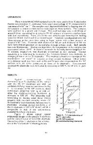
Comparative morphology of AuTiAlTi, AuPdAlTi and AuAlTi ohmic contacts to AlGaN/GaN M W Fay, G Moldovan, I Harrison1, R.S. Balmer2, K P Hilton2, B T Hughes2, M J Uren2, T Martin2 and P D Brown School of Mechanical, Materials, Manufacturing Engineering and Management, University of Nottingham, University Park, Nottingham NG7 2RD, UK 1 School of Electrical and Electronic Engineering, University of Nottingham, University Park, Nottingham NG7 2RD, UK 2 QinetiQ Ltd, St Andrews Rd, Malvern, Worcs WR14 3PS, UK ABSTRACT AuTiAlTi, AuPdAlTi and AuAlTi ohmic contacts to AlGaN/GaN layers rapid thermal annealed at temperatures up to 950°C have been characterised using conventional and chemical transmission electron microscopy techniques. The relationship between the as-deposited metallic structure, annealing temperature, post-anneal interfacial microstructure and contact resistance is examined. The presence of a TiN interfacial layer is found to correlate with the onset of ohmic behaviour. Ti and Pd barrier layers are found to be ineffective at stopping the diffusion of Au to the interface. Au is implicated in the development of the inclusions, which are associated with threading dislocations. Once activated, the presence of the inclusions has little influence on the ohmic behaviour of the sample. INTRODUCTION Devices based on AlGaN/GaN heterostructures are of great interest in the area of high power, high frequency applications. Reproducible, low resistance ohmic contacts are required for such applications. Ohmic contacts to n-type GaN and AlGaN are normally based on the reaction of an Al/Ti diffusion couple to form an intermetallic Ti:Al –based layer, with an interfacial Ti-nitride layer and a nitrogen depletion layer at the semiconductor surface to activate the contact. As Al and Ti layers are both susceptible to oxidation, Au capping layers are used as an oxidation resistant material, and to planarise the contact to assist with wire bonding. It was considered undesirable to have Au diffusing to the contact/nitride interface [1], and so diffusion barrier layers of materials such as Ti, Pd, Ni and Pt were introduced within the Au/Al/Ti contact scheme. [2,3,4,5]. However, TEM analysis of such layers indicate that they are ineffective at preventing the diffusion of Au to the semiconductor, and it has more recently been suggested that this may not actually be undesirable [6] A large number of variables affect the characteristics of a metal diffusion couple contact, including the nature of the GaN wafer, which makes it difficult to compare results published in the literature. It is preferable to compare samples with a single variable altered, processed on the same GaN wafer. In this paper, we consider three contact schemes, typical of multilayer contacts reported in the literature, to AlGaN/GaN.
L11.55.2
EXPERIMENTAL METHOD Firstly, a 300nm Au / 60nm Ti / 100nm Al / 20nm Ti contact to AlGaN/GaN grown by metal organic chemical vapour deposition (MOCVD) on a sapphire substrate with samples annealed at temperatures from
Data Loading...